English
 Español
 tiếng việt
 русский
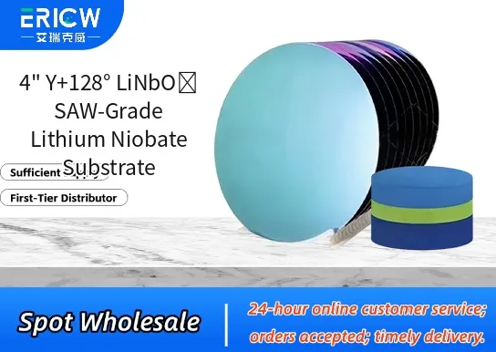
Optimized crystal cut (Y+128°) for high electromechanical coupling coefficient (K² ≈ 5.5%) and low temperature coefficient of delay (TCD) in surface acoustic wave (SAW) devices.
Ultra-low surface roughness (<0.3 nm RMS) achieved via precision lapping, polishing, and cleaning—ensuring minimal insertion loss and high-frequency stability.
SAW-grade purity with controlled stoichiometry and low defect density (dislocation density < 1 × 10⁴ cm⁻²), validated by X-ray topography and etch pit density (EPD) analysis.
Standard 4-inch (100 mm) diameter with ±0.1 mm tolerance, 0.5 mm nominal thickness, and laser-scribed orientation flats for automated handling in fab environments.
Chemically stable under standard cleanroom processing (RCA, piranha, BOE), with no lithium out-diffusion or surface degradation during metallization or annealing up to 300 °C.
High-performance RF SAW filters and duplexers for 5G mobile front-end modules (FEMs) operating up to 3.8 GHz.
Temperature-stable resonators and sensors in industrial IoT systems requiring ±10 ppm/°C frequency stability over −40 °C to +85 °C.
Low-loss delay lines and signal processors in aerospace radar and electronic warfare (EW) subsystems.
Integrated piezoelectric micro-machined ultrasonic transducers (PMUTs) for wearable biomedical imaging platforms.
Research-grade substrates for thin-film lithium niobate (TFLN) hybrid integration and electro-optic modulator development.
| Chemical Type | Lithium Niobate (LiNbO₃), congruent composition |
| Product Form | Single-crystal wafer, double-side polished |
| Crystal Orientation | Y-axis rotated +128° about X-axis (Y+128°) |
| Diameter & Tolerance | 100.0 ± 0.1 mm |
| Thickness & Tolerance | 0.500 ± 0.010 mm |
| Surface Roughness (Ra) | ≤ 0.3 nm (both sides, measured by AFM) |
| Primary Applications | Surface Acoustic Wave (SAW) device fabrication |
| Regulatory Compliance | RoHS 2015/863/EU compliant; REACH SVHC-free (verified by ICP-MS) |
| Common Compatible Systems | Suitability |
| Applied Materials ENDURA® iLB Line | Highly Recommended – Optimized for Ti/Pt/Au sputtering and lift-off on Y+128° LiNbO₃ wafers |
| EV Group EVG® 620 Mask Aligner | Highly Recommended – Verified alignment accuracy < 0.5 µm using flat/notch registration |
| Screen Printing Systems (e.g., DEK Horizon) | Recommended – Compatible with Ag/Pd thick-film pastes for low-frequency SAW interdigital transducers (IDTs) |
| Plasma Etch Tools (Oxford Plasmalab System 100) | Suitable – Requires CHF₃/O₂ chemistry for selective LiNbO₃ patterning; etch rate ~15 nm/min |
Q1: What is the CAS Registry Number for lithium niobate (LiNbO₃)?
A: The CAS Registry Number for lithium niobate is 12031-63-3.
Q2: Is lithium leaching or ion migration observed under typical SAW device operating conditions?
A: No significant lithium migration occurs below 300 °C and at RF power densities ≤ 1 W/mm². Accelerated life testing (1000 hrs @ 85 °C, 85% RH) shows no measurable Li⁺ extraction into polymer encapsulants per ASTM D1388.
Q3: How does Y+128° LiNbO₃ compare to ST-Quartz or 42° YX-LiTaO₃ for high-frequency SAW filters?
A: Y+128° LiNbO₃ offers ~2× higher K² than ST-Quartz and ~1.4× higher than 42° YX-LiTaO₃, enabling broader bandwidth and smaller device footprints—but requires tighter process control due to lower acoustic velocity.
Q4: Does this substrate meet ISO 10993 biocompatibility requirements?
A: While not certified for implantation, the material complies with ISO 10993-5 (cytotoxicity) and ISO 10993-12 (sample preparation) for short-term external-contact applications; full biocompatibility assessment requires end-device-level testing.
Contact With Us:
E-mail: wangxingqiang@ericwchem.com
Have a Questions? Call Us:
Add:
Building A1, Jiete Industrial Park, Huangpu District, Guangzhou City, Guangdong Province, China