English
 Español
 tiếng việt
 русский
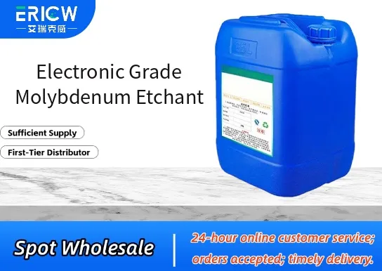
Ultra-low metallic impurity profile (≤10 ppt for Na, K, Fe, Cu, Ni, Cr, Zn, and Ca), meeting SEMI C12 and ASTM F2287 standards for electronic-grade processing.
Controlled etch rate uniformity (<±3% across 300 mm wafers) enabled by precise pH buffering and stabilizer system.
Non-oxidizing formulation minimizes interfacial oxidation of underlying TiN or TaN barrier layers during Mo film removal.
Compatible with standard photoresist stripping chemistries—no cross-contamination or residue formation observed in dual-damascene integration flows.
Stable shelf life (>24 months unopened at 15–25°C) with no phase separation or precipitate formation under recommended storage conditions.
Etching of molybdenum (Mo) thin films in advanced logic and memory device fabrication (e.g., gate electrodes, interconnect seed layers).
Back-end-of-line (BEOL) patterning of Mo-based resistive switching layers in emerging ReRAM and neuromorphic memory stacks.
Selective removal of Mo capping layers prior to Cu electroplating in hybrid metallization schemes.
Wafer-level packaging (WLP) processes requiring ultra-clean Mo etch for redistribution layer (RDL) interconnects.
MEMS and RF front-end module fabrication where Mo is used as a high-melting-point structural or electrode material.
| Chemical Type | Aqueous acidic solution (non-hydrofluoric, non-peroxide) |
| Product Form | Liquid concentrate (ready-to-use after dilution with UPW) |
| Appearance | Clear, colorless to pale yellow liquid |
| pH (as supplied) | 1.8–2.2 at 25°C |
| Density (25°C) | 1.04–1.07 g/cm³ |
| Primary Applications | Wet etching of Mo films (2–500 nm thickness) on Si, SiO₂, SiN, TiN, and low-k dielectrics |
| Key Features | High Mo selectivity vs. TiN (>120:1), SiO₂ (>250:1), and photoresist (>80:1) |
| Regulatory Compliance | REACH SVHC-free; RoHS 3 compliant; no intentionally added PFAS |
| Common Compatible Systems | Suitability |
| SEZ® / SCREEN® Wet Processing Tools (e.g., AURA™, SPRINT™) | Highly Recommended – Fully validated for single-wafer spray and immersion modes with real-time temperature & flow control |
| TEL® ACT™ Series (ACT 8/12) | Recommended – Requires minor process parameter tuning; compatible with standard chemical delivery modules |
| Applied Materials® Eterna™ Wet Etch Platforms | Suitable – Functional with standard UPW dilution kits; etch uniformity meets <±4% spec |
| Manual benchtop dip tanks (quartz or PFA-lined) | Suitable – Validated for R&D and low-volume pilot lines using controlled immersion time (30–120 s) |
Q1: What is the CAS Registry Number for this etchant?
A: This is a proprietary multi-component formulation; individual CAS numbers are not assigned to the final product. Key constituents include ammonium nitrate (CAS 6484-52-2), phosphoric acid (CAS 7664-38-2), and chelated organic acids (CAS 61789-40-0). Full ingredient disclosure is available under NDA.
Q2: What is the recommended working concentration and typical etch rate?
A: Dilute 1:4 to 1:9 (v/v) with 18.2 MΩ·cm ultrapure water (UPW). At 25°C and 1:5 dilution, typical etch rate for 50-nm sputtered Mo on SiO₂ is 32–38 Å/s, with <±2.5% within-wafer uniformity.
Q3: How does it compare to traditional HF/HNO₃-based Mo etchants?
A: Unlike aggressive HF/HNO₃ mixtures, this etchant eliminates silicon substrate attack, prevents nitride layer degradation, and requires no special ventilation for NOₓ fumes. It also enables higher Mo:TiN selectivity (>120:1 vs. <20:1) and reduces particle generation by >90% per wafer.
Q4: Are there any known metal ion migration or leaching concerns into low-k dielectrics?
A: No measurable Mo, Ni, or Fe migration into porous SiCOH (k=2.7) was detected after 60-s exposure at 30°C (ICP-MS analysis, detection limit 0.05 ppq). The chelating system effectively suppresses free metal ion activity.
Q5: Does the product require special handling certifications (e.g., ISO 14644-1 Class 1 cleanroom compatibility)?
A: Yes — manufactured and packaged in ISO 14644-1 Class 1 environment; certified for use in Class 10 (ISO 4) cleanrooms. Certificate of Analysis includes particle count data (≤1 particle/mL ≥0.1 µm per USP <788> method).
Contact With Us:
E-mail: wangxingqiang@ericwchem.com
Have a Questions? Call Us:
Add:
Building A1, Jiete Industrial Park, Huangpu District, Guangzhou City, Guangdong Province, China