English
 Español
 tiếng việt
 русский
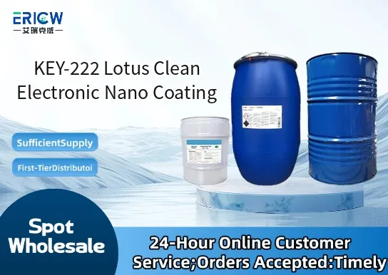
Ultra-thin, transparent nanoscale film (≤100 nm thickness) that preserves original surface aesthetics and optical clarity.
Hydrophobic and oleophobic surface protection with contact angle >110° for water and >75° for oils.
Room-temperature curing formulation—no thermal baking or UV activation required.
Non-conductive, dielectric coating (volume resistivity >1×10¹² Ω·cm) safe for sensitive electronic components.
Halogen-free, solvent-based system compliant with IPC-CC-830B Class A requirements for electronic conformal coatings.
Protection of printed circuit boards (PCBs), sensors, and MEMS devices against humidity, condensation, and ionic contamination.
Surface treatment for touchscreens, OLED displays, and automotive HMI interfaces to enhance smudge resistance and cleanability.
Coating of precision connectors, RF antennas, and battery management system (BMS) modules to prevent corrosion and dendrite formation.
Preventive barrier layer for medical electronics (e.g., diagnostic handhelds, wearable monitors) exposed to alcohol-based disinfectants.
Nano-protection for IoT edge devices operating in high-humidity or coastal environments.
| Chemical Type | Fluorinated silane hybrid nano-solution |
| Product Form | Clear, low-viscosity liquid (solvent-based) |
| Appearance | Colorless to pale yellow, homogeneous solution |
| Primary Applications | Electronic component surface protection, anti-fouling barrier, moisture resistance enhancement |
| Key Features | Room-temperature self-assembly, covalent Si–O–substrate bonding, no post-cure needed |
| Benefits | Reduces surface energy, inhibits fingerprint adhesion, improves wipe-clean performance, maintains signal integrity |
| Regulatory Compliance | RoHS 2015/863 compliant; REACH SVHC-free; IPC-CC-830B Class A qualified |
| Storage Stability | 12 months unopened at 5–25°C; protect from direct sunlight and moisture |
| Common Compatible Systems | Suitability |
| Glass, quartz, and sapphire substrates | Highly Recommended – Forms robust covalent bonds via surface hydroxyl groups |
| Aluminum oxide (Al₂O₃), anodized aluminum, and stainless steel | Recommended – Requires light plasma or chemical pre-treatment for optimal adhesion |
| FR-4 PCB laminates and solder mask (epoxy/acrylic) | Suitable – Adheres well; verify compatibility with specific solder mask chemistry via patch test |
| Polyimide flex circuits and PET touch sensor films | Recommended – Compatible with standard dip/spray processes; avoid prolonged solvent exposure |
Q1: What is the CAS Registry Number for KEY-222 Lotus Clean Electronic Nano Coating?
A: KEY-222 is a proprietary multi-component formulation; individual active ingredients include CAS 13429-28-4 (perfluoroalkylsilane derivative) and CAS 68441-17-8 (functional siloxane oligomer). Full composition is protected under trade secret; SDS discloses all reportable constituents.
Q2: What is the recommended application dosage and coverage rate?
A: Typical usage is 8–12 mL/m² via spray, dip, or spin-coating. One liter covers approximately 85–125 m² depending on substrate porosity and process efficiency. Achieves functional monolayer coverage at ~0.3–0.5 g/m² dry film weight.
Q3: How does KEY-222 compare to conventional acrylic or silicone conformal coatings?
A: Unlike thick polymer coatings (≥25 µm), KEY-222 forms a sub-100 nm molecular layer—preserving dimensional tolerance, thermal conductivity, and high-frequency signal transmission. It offers superior chemical resistance vs. acrylics and avoids silicone migration issues common in RF-sensitive assemblies.
Q4: Is KEY-222 subject to extractable or leachable concerns per ISO 10993 or USP <87>?
A: Migration testing per USP <87> (in vitro cytotoxicity) and ISO 10993-5 shows no detectable leachables or cytotoxic response under standard extraction conditions (simulated body fluid, 72h, 37°C). Residual solvent levels fall below ICH Q3C Stage 3 limits.
Q5: Does KEY-222 require special handling for ESD-safe environments?
A: Yes—KEY-222 is formulated with static-dissipative solvents and yields a surface resistivity of 10⁹–10¹¹ Ω/sq after curing, meeting ANSI/ESD S20.20 requirements for EPA use without additional grounding measures.
Contact With Us:
E-mail: wangxingqiang@ericwchem.com
Have a Questions? Call Us:
Add:
Building A1, Jiete Industrial Park, Huangpu District, Guangzhou City, Guangdong Province, China