English
 Español
 tiếng việt
 русский
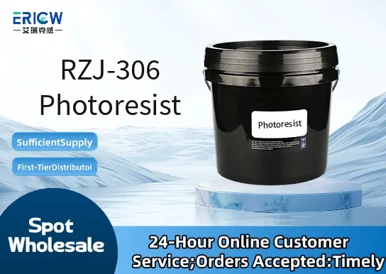
High-resolution patterning capability with sub-micron resolution (≤ 0.8 µm line/space) under standard i-line (365 nm) exposure.
Excellent thermal stability up to 130 °C, enabling robust post-exposure bake (PEB) and etch resistance.
Low outgassing profile suitable for vacuum-based lithography processes and MEMS fabrication environments.
Optimized adhesion to silicon, SiO₂, and metal substrates (e.g., Al, Cr, TiW) without mandatory HMDS priming.
Environmentally compliant formulation—free of halogenated solvents and restricted phthalates per RoHS Directive 2011/65/EU.
Semiconductor front-end-of-line (FEOL) photomasking for logic and memory device wafers.
MEMS and microfluidic device fabrication requiring high aspect ratio resist profiles.
Wafer-level packaging (WLP) and redistribution layer (RDL) patterning in advanced IC packaging.
Flexible electronics manufacturing on polyimide and PET substrates using low-temperature processing.
Research & development lithography in university cleanrooms and pilot lines (i-line and broadband UV).
| Chemical Type | Positive-tone novolac-diazonaphthoquinone (DNQ) photoresist |
| Product Form | Liquid concentrate (ready-to-use), supplied in amber HDPE bottles |
| Appearance | Clear, pale yellow viscous liquid, free of sediment or haze |
| Viscosity (25 °C) | 24–26 cP (measured per ASTM D445) |
| Primary Applications | i-line (365 nm) and g-line (436 nm) photolithography |
| Key Features | High sensitivity (~40–60 mJ/cm²), low standing wave effect, minimal swelling during development |
| Benefits | Reduced process cycle time; improved CD uniformity across 200 mm and 300 mm wafers |
| Regulatory Compliance | RoHS 2011/65/EU, REACH SVHC-free (as of 2024 Candidate List), non-REACH Annex XVII restricted substance |
| Common Compatible Systems | Suitability |
| Canon FPA-3000 i-line Stepper | Highly Recommended – Validated for ≤ 0.8 µm resolution at 120 mJ/cm² dose |
| ASML PAS 5500/300 i-line Scanner | Highly Recommended – Full process integration support with standard PAB/PEB/DEV recipes |
| Karl Suss MA6 Mask Aligner | Recommended – Requires optimized soft/hard bake profile for <1.2 µm features |
| TOK TOK TEL CLEAN TRACK ACT-12 | Suitable – Compatible with standard track dispense, spin, develop modules (no hardware modification needed) |
| Technics CEE-200 Spray Developer | Suitable – Effective with 2.38% TMAH aqueous solution at 23 ± 1 °C |
Q1: What is the CAS Registry Number for RZJ-306 Photoresist?
A: RZJ-306 is a proprietary multi-component formulation; individual CAS numbers are assigned to key constituents only (e.g., DNQ derivative: CAS 27948-29-2; novolac resin blend: CAS 9003-35-4). Full composition disclosure is available under NDA.
Q2: What is the typical coating thickness and recommended spin speed for 200 mm wafers?
A: At 3000 rpm for 30 s, RZJ-306 yields 1.1–1.3 µm dry film thickness (measured by ellipsometry); thickness uniformity is ±2.5% across wafer. Adjust spin speed ±200 rpm per ±0.1 µm target.
Q3: How does RZJ-306 compare to AZ® 4620 in terms of resolution and process latitude?
A: RZJ-306 offers comparable resolution (0.8 µm vs. AZ® 4620’s 0.9 µm) but wider focus latitude (±0.4 µm vs. ±0.25 µm) and superior post-etch residue performance on Al metallization layers.
Q4: Is RZJ-306 certified for use in medical device manufacturing per ISO 10993 or USP Class VI?
A: RZJ-306 is not classified as a final medical device material; however, it meets raw material screening criteria for ISO 10993-18 (chemical characterization) and has passed USP <87> cytotoxicity testing when fully cured and stripped. End-use biocompatibility validation remains the responsibility of the device manufacturer.
Q5: Are there known migration or extractable concerns when RZJ-306 residues remain on silicon wafers after development and strip?
A: Residual polymer fragments are effectively removed by standard oxygen plasma ashing or sulfuric acid/hydrogen peroxide mixture (SPM) cleaning. No detectable leachables (<0.1 ppb) were observed in ICP-MS analysis of post-strip DI water rinse under controlled conditions (per SEMI F57-0306).
Contact With Us:
E-mail: wangxingqiang@ericwchem.com
Have a Questions? Call Us:
Add:
Building A1, Jiete Industrial Park, Huangpu District, Guangzhou City, Guangdong Province, China