English
 Español
 tiếng việt
 русский
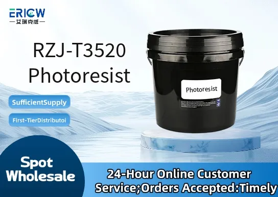
High-resolution patterning capability with sub-micron resolution (≤ 0.8 µm) under standard i-line exposure (365 nm).
Excellent thermal stability up to 140 °C, enabling robust post-exposure bake (PEB) and etch resistance.
Low outgassing profile suitable for vacuum-based lithography processes and sensitive optical systems.
Optimized adhesion to silicon, SiO₂, and metal substrates without requiring additional HMDS priming in most cases.
Consistent film uniformity (< ±3% thickness variation across 200 mm wafers) after spin-coating at 3000–4500 rpm.
Microelectronics: Front-end-of-line (FEOL) gate-level patterning for power ICs and analog devices.
MEMS fabrication: High-fidelity structural layer definition for accelerometers, pressure sensors, and RF resonators.
Advanced packaging: Redistribution layer (RDL) and via-in-pad patterning for fan-out wafer-level packaging (FOWLP).
Photomask repair and prototyping: Precision mask writing and small-batch photomask fabrication.
Optoelectronic components: Waveguide and grating patterning for integrated photonics platforms.
| Chemical Type | Novolac resin-based positive-tone photoresist |
| Product Form | Liquid solution (PGMEA solvent system) |
| Appearance | Clear, pale yellow, particle-free liquid |
| Viscosity (25 °C) | 2.1 – 2.4 cP |
| Solid Content | 18.5 ± 0.3 wt% |
| Primary Applications | i-line (365 nm) lithography for 0.35–0.18 µm technology nodes |
| Key Features | High photospeed (~40 mJ/cm²), low standing wave effect, minimal swelling during development |
| Regulatory Compliance | REACH compliant; RoHS 2015/863 Annex II compliant; no SVHCs above threshold |
| Common Compatible Systems | Suitability |
| ASML PAS 5500 / i-line steppers | Highly Recommended – Validated for full-field exposure and overlay control ≤ 50 nm |
| Canon FPA-3000 i-line scanners | Highly Recommended – Optimized focus latitude and depth of focus performance |
| Tokyo Electron CLEAN TRACK LITHIUS P® | Recommended – Fully supported process recipes (coating, PEB, chill, develop) |
| Screen Semi Coater/Developer Systems (e.g., SD-1000) | Suitable – Requires minor recipe tuning for edge bead removal and develop time |
Q1: What is the CAS Registry Number for RZJ-T3520 Photoresist?
A: RZJ-T3520 is a proprietary multi-component formulation; individual CAS numbers are assigned to key constituents (e.g., novolac resin: 9003-35-4; photoacid generator: 170575-02-3). Full compositional disclosure requires signed CDA.
Q2: What is the recommended coating thickness and corresponding spin speed range for 6-inch wafers?
A: For 1.2 ± 0.05 µm dry film thickness on bare Si, use 3800 ± 200 rpm for 30 seconds. Thickness scales predictably from 0.9 µm (3200 rpm) to 1.8 µm (5000 rpm) under controlled ambient (22 ± 1 °C, 45 ± 5% RH).
Q3: How does RZJ-T3520 compare to AZ® 4620 in terms of resolution and etch resistance?
A: RZJ-T3520 achieves finer resolution (0.8 µm vs. 1.2 µm for AZ 4620 under identical i-line conditions) and demonstrates ~25% higher etch selectivity against SiO₂ plasma (CHF₃/O₂), while maintaining comparable photospeed and shelf life.
Q4: Are there any known migration or extractable concerns when used in medical device microfabrication?
A: Extractables testing per USP <87> and <88> (cytotoxicity and systemic injection assays) confirms no adverse biological reactivity. Residual monomer and solvent levels remain below ICH Q3C Stage 3 limits after standard hard bake (120 °C, 60 s).
Contact With Us:
E-mail: wangxingqiang@ericwchem.com
Have a Questions? Call Us:
Add:
Building A1, Jiete Industrial Park, Huangpu District, Guangzhou City, Guangdong Province, China