English
 Español
 tiếng việt
 русский
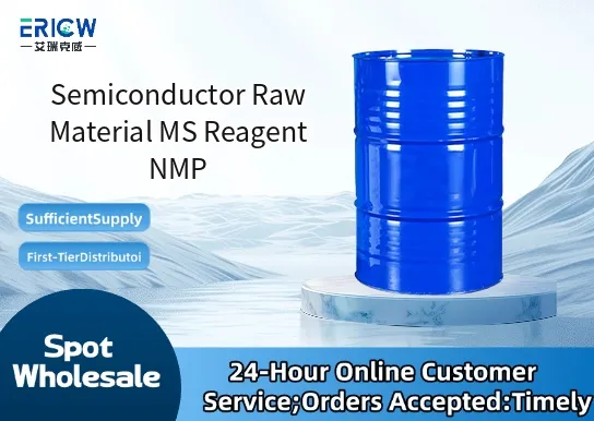
Ultra-high purity grade (≥99.9% GC), specifically refined to meet semiconductor-grade solvent specifications with stringent metal ion control (Na, K, Fe, Cu < 10 ppb).
Low residual water content (<50 ppm) to prevent hydrolysis during photoresist formulation and spin-coating processes.
Controlled peroxide formation inhibitors and nitrogen blanketed packaging to ensure long-term stability and consistent performance in cleanroom environments.
Batch-certified traceability with full CoA (Certificate of Analysis) including ICP-MS metals profile and GC chromatogram.
Non-halogenated, non-corrosive, and compatible with stainless steel and fluoropolymer fluid handling systems.
Primary solvent for high-resolution positive and negative tone photoresists used in advanced lithography (i-line, KrF, ArF).
Carrier medium for polyimide precursor solutions in flexible printed circuit (FPC) and chip-on-film (COF) manufacturing.
Stripping agent in post-etch and post-ash residue removal for copper/low-k interconnect integration.
Processing aid in chemical mechanical planarization (CMP) slurry formulation for barrier layer polishing.
Solvent for conductive polymer dispersions (e.g., PEDOT:PSS) in next-generation display driver IC packaging.
| Chemical Type | N-Methyl-2-pyrrolidone (NMP), organic polar aprotic solvent |
| Product Form | Liquid, clear, colorless |
| Appearance | Clear, transparent, free from suspended particles or haze |
| Melting Point | −24 °C |
| Boiling Point (760 mmHg) | 202 °C |
| Primary Applications | Photoresist formulation, polyimide processing, resist stripping, CMP additive carrier |
| Key Features | High dielectric constant (ε ≈ 32), excellent solvating power, low volatility at room temperature |
| Regulatory Compliance | REACH registered; RoHS compliant; no SVHCs above threshold; SDS available per ISO 11014 |
| Common Compatible Systems | Suitability |
| ASML NXT Lithography Track Systems (e.g., NXT:1980Di) | Highly Recommended – Validated for resist dispense and develop modules under Class 10 cleanroom conditions |
| Tokyo Electron (TEL) CLEAN TRACK® LITHIUS+ | Highly Recommended – Pre-qualified for NMP-based resist coating and post-apply bake sequences |
| Screen Semi R&D Dispensing Platforms | Recommended – Compatible with precision microdispense valves using PTFE and EPDM wetted materials |
| Dainippon Screen (DNS) SPRINT™ Etch & Strip Tools | Suitable – Confirmed for use in low-temperature strip chemistry delivery lines with corrosion-resistant flow paths |
Q1: What is the CAS number for Semiconductor Raw Material MS Reagent NMP?
A: The CAS Registry Number is 872-50-4. Each production batch is verified via FTIR and GC-MS against this reference standard.
Q2: What is the recommended usage concentration when formulating photoresists?
A: Typical formulations use 85–95 wt% NMP as the primary solvent phase. Final concentration must be validated per resist polymer Tg and process viscosity requirements—never exceed 98 wt% without compatibility testing.
Q3: How does MS Reagent NMP differ from technical-grade or electronics-grade NMP?
A: MS Reagent NMP undergoes additional sub-micron filtration, multi-stage molecular distillation, and real-time metal monitoring—achieving ≤10 ppb total metals vs. ≥100 ppb in standard electronics grade—critical for sub-7nm node defect control.
Q4: Is migration or leaching into silicon wafers a concern during high-temperature processing?
A: No measurable NMP residue remains after standard post-apply bake (PAB) at ≥90 °C for 60 sec. FTIR and TOF-SIMS confirm complete volatilization; residual carbon content is below detection limit (<0.001 monolayer).
Contact With Us:
E-mail: wangxingqiang@ericwchem.com
Have a Questions? Call Us:
Add:
Building A1, Jiete Industrial Park, Huangpu District, Guangzhou City, Guangdong Province, China