English
 Español
 tiếng việt
 русский
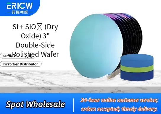
High-purity silicon substrate with thermally grown dry SiO₂ layer (100–200 nm nominal thickness) for superior interface quality and low defect density.
Double-side polished surface achieving Ra < 0.2 nm on both sides, enabling high-precision lithography and bonding processes.
Dry oxidation process ensures stoichiometric SiO₂ with minimal hydrogen content and excellent dielectric uniformity (±2% thickness variation across wafer).
3-inch diameter (76.2 mm) standard wafer format compatible with legacy and R&D semiconductor tooling.
Controlled oxygen vacancy profile and low fixed oxide charge (< 5 × 10¹⁰ cm⁻²), optimized for MOS capacitor and sensor fabrication.
Silicon-based MEMS device prototyping, including pressure sensors and accelerometers.
R&D platform for gate dielectric evaluation in novel transistor architectures (e.g., GAA, TFET).
Substrate for thin-film deposition studies (ALD, PECVD) requiring atomically clean, thermally stable SiO₂ surfaces.
Calibration and reference wafers in surface metrology (AFM, ellipsometry, XRR) labs.
Fabrication of microfluidic lab-on-a-chip devices with integrated oxide insulation layers.
| Chemical Composition | Single-crystal Czochralski (CZ) silicon substrate + thermally grown SiO₂ (dry O₂ ambient) |
| Product Form | Round wafer, 3-inch (76.2 mm) diameter, double-side polished |
| SiO₂ Thickness (Nominal) | 150 nm ± 5 nm (measured by spectroscopic ellipsometry) |
| Surface Roughness (Ra) | < 0.2 nm (both sides, measured by AFM over 10 × 10 µm²) |
| Crystal Orientation | (100) ± 0.5° |
| Resistivity Range | 1–10 Ω·cm (N-type, phosphorus-doped) |
| Primary Applications | Semiconductor R&D, MEMS prototyping, surface science, thin-film process development |
| Regulatory Compliance | RoHS 2015/863 compliant; REACH SVHC-free; no intentional PFAS or heavy metal additives |
| Common Compatible Systems | Suitability |
| JEOL JSM-7800F SEM / EDS Platform | Highly Recommended – Ideal for high-resolution imaging and quantitative oxide layer analysis |
| Horiba UVISEL2 Spectroscopic Ellipsometer | Highly Recommended – Optimized for accurate SiO₂ thickness and optical constant extraction |
| Applied Materials ENDURA® Platform (with PVD modules) | Recommended – Compatible with oxide surface pretreatment and metallization steps |
| Canon FPA-3030i5a Stepper (3-inch adapter) | Suitable – Supports alignment and exposure with standard 3-inch wafer chucks and fiducials |
Q1: Does this product have a CAS number?
A: Silicon (CAS 7440-21-3) and silicon dioxide (CAS 7631-86-9) are listed separately; however, this is a physical composite structure—not a chemical compound—so no unified CAS number is assigned per IUPAC and regulatory guidelines.
Q2: What is the recommended storage condition to preserve oxide integrity?
A: Store in Class 100 cleanroom environment at 20–25°C and 30–50% RH, inside nitrogen-purged, static-dissipative wafer carriers; avoid prolonged ambient exposure (>4 hours) prior to processing.
Q3: How does dry oxide compare to wet oxide in terms of breakdown field and interface trap density?
A: Dry oxide exhibits higher dielectric strength (~10 MV/cm vs. ~6–8 MV/cm for wet oxide) and lower interface trap density (Dit ≈ 1×10¹⁰ eV⁻¹cm⁻² at mid-gap) due to reduced hydrogen incorporation and slower growth kinetics.
Q4: Is leachable silicon or silica detectable under standard aqueous extraction protocols (e.g., USP <661.1>)?
A: No measurable leachables are observed under USP <661.1> simulated extraction conditions (water, 50°C, 24 h); the thermally grown SiO₂ layer is chemically inert and non-porous, with negligible ion release (<0.1 ppb Si by ICP-MS).
Contact With Us:
E-mail: wangxingqiang@ericwchem.com
Have a Questions? Call Us:
Add:
Building A1, Jiete Industrial Park, Huangpu District, Guangzhou City, Guangdong Province, China