English
 Español
 tiếng việt
 русский
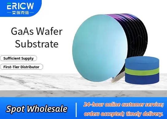
Single-crystal gallium arsenide (GaAs) wafers with high structural uniformity and low dislocation density (< 5 × 10³ cm⁻²).
Available in standard diameters (2", 3", 4", 6") and thicknesses (250–625 µm), polished on both sides (e.g., SSP/ DSP) with controlled surface roughness (< 0.3 nm RMS).
High electron mobility and superior semi-insulating or n-type/p-type doping options (e.g., SI-Cr, Si-doped, Zn-doped) for tailored electrical performance.
Thermal stability up to 600 °C in inert environments, enabling compatibility with high-temperature epitaxial growth processes (e.g., MBE, MOCVD).
Low oxygen and carbon contamination levels, verified via secondary ion mass spectrometry (SIMS), ensuring high device yield in RF and optoelectronic fabrication.
High-frequency radio frequency (RF) and microwave integrated circuits (MICs, MMICs) for 5G infrastructure and radar systems.
High-efficiency photovoltaic cells, including multi-junction solar cells for space and concentrated photovoltaics (CPV).
Vertical-cavity surface-emitting lasers (VCSELs), edge-emitting lasers (EELs), and infrared light-emitting diodes (LEDs).
Heterojunction bipolar transistors (HBTs) and pseudomorphic high-electron-mobility transistors (pHEMTs) for low-noise amplification.
Sensors and quantum devices requiring direct-bandgap semiconductor properties and radiation hardness.
| Chemical Type | Gallium Arsenide (GaAs), ultra-high-purity single crystal |
| Product Form | Polished circular wafer (double-side polished, optional etch-back or EPD-tested) |
| Crystal Orientation | (100) ± 0.5°, with primary flat (or notch) per SEMI standards |
| Resistivity (SI Grade) | > 1 × 10⁸ Ω·cm (Cr-compensated, semi-insulating) |
| Carrier Concentration (n-type) | 1 × 10¹⁷ – 5 × 10¹⁸ cm⁻³ (Si-doped, controllable) |
| Surface Finish | Chemomechanical polish (CMP) with < 0.2 nm RMS roughness (per AFM) |
| Primary Applications | Epitaxial growth substrates for III-V compound semiconductors (e.g., AlGaAs, InGaAs) |
| Regulatory Compliance | RoHS-compliant; no intentionally added REACH SVHC substances; trace metal impurities < 1 × 10¹⁶ cm⁻³ (SIMS-verified) |
| Common Compatible Systems | Suitability |
| MBE (Molecular Beam Epitaxy) Systems (e.g., Riber, Veeco) | Highly Recommended – Optimized for oxide desorption and stable As-stabilized surface reconstruction |
| MOCVD (Metalorganic Chemical Vapor Deposition) Systems (e.g., AIXTRON, Thomas Swan) | Highly Recommended – Compatible with standard AsH₃/TMGa precursors and thermal ramp profiles |
| Ion Implantation Tools (e.g., Axcelis, Varian) | Recommended – Supports shallow junction formation with minimal channeling due to (100) orientation |
| Wafer Bonding Platforms (e.g., EV Group EVG620) | Suitable – Achieves > 95% bonding strength with SiO₂ or Si handles under optimized surface activation |
Q1: What is the CAS Number for Gallium Arsenide?
A: The CAS Registry Number for gallium arsenide is 1303-00-0.
Q2: Is GaAs wafer substrate subject to leaching or elemental migration under processing conditions?
A: GaAs is chemically stable under standard cleanroom handling and dry etching. However, acidic or oxidizing wet chemistries (e.g., HCl/H₂O₂, Br-based solutions) may cause measurable As or Ga release; use only certified semiconductor-grade etchants with strict process controls.
Q3: How does GaAs compare to silicon or SiC substrates for high-frequency applications?
A: GaAs offers higher electron mobility (~8500 cm²/V·s vs. ~1400 cm²/V·s for Si) and superior semi-insulating properties versus doped Si, enabling lower parasitic capacitance and higher fₜ/fₘₐₓ—making it preferred for mmWave RF and optoelectronic integration where SiC’s thermal advantage is less critical.
Q4: Does your GaAs wafer substrate carry ISO 9001 or IATF 16949 certification?
A: All GaAs wafer substrates are manufactured in ISO 9001:2015-certified cleanrooms; IATF 16949 applies to automotive-grade wafers upon request and subject to additional qualification testing (e.g., AEC-Q200 screening).
Contact With Us:
E-mail: wangxingqiang@ericwchem.com
Have a Questions? Call Us:
Add:
Building A1, Jiete Industrial Park, Huangpu District, Guangzhou City, Guangdong Province, China