English
 Español
 tiếng việt
 русский
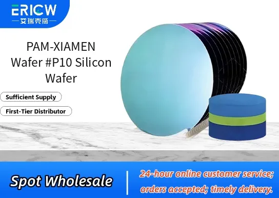
High-purity monocrystalline silicon substrate with resistivity control in the 1–10 Ω·cm range.
Double-side polished surface achieving Ra < 0.2 nm for optimal thin-film deposition and lithography performance.
Available in standard diameters (100 mm, 150 mm) with tight thickness uniformity (±5 µm tolerance).
Oxide-ready surface with native SiO₂ layer ≤ 1.5 nm, compatible with thermal oxidation and cleaning protocols.
ISO Class 5 cleanroom processed and individually packaged in nitrogen-purged, static-dissipative cassettes.
Semiconductor device prototyping and R&D for CMOS, MEMS, and power electronics.
Photovoltaic cell research including passivated emitter rear contact (PERC) and heterojunction (HJT) structures.
Microfabrication of lab-on-a-chip sensors and integrated optical waveguides.
Calibration and reference substrates in surface analysis tools (XPS, AFM, ellipsometry).
Thin-film transistor (TFT) backplane development for flexible display and sensor applications.
| Chemical Type | Monocrystalline Silicon (Si) |
| Crystal Orientation | (100) ± 0.5° |
| Diameter | 100 mm (4-inch) or 150 mm (6-inch), selectable |
| Thickness | 525 ± 10 µm (100 mm); 675 ± 10 µm (150 mm) |
| Surface Finish | Double-Side Polished (DSP), front: epi-ready, back: etch-stop compatible |
| Resistivity Range | 1–10 Ω·cm (Phosphorus-doped, N-type) |
| Primary Applications | Semiconductor R&D, MEMS fabrication, photovoltaic testing, academic microfabrication |
| Regulatory Compliance | RoHS 2015/863 compliant; REACH SVHC-free; no intentional PFAS use |
| Common Compatible Systems | Suitability |
| KLA-Tencor P-17 Profilometer | Highly Recommended – Verified step-height repeatability < ±0.3 nm |
| Applied Materials Endura® Platform | Highly Recommended – Validated for Ti/TiN/PVD seed layer adhesion |
| ASM International Phoenix™ LPCVD System | Recommended – Compatible with SiO₂ and Si₃N₄ deposition at 650–800°C |
| Oxford Instruments Plasmalab® System | Suitable – Supports ICP-RIE etching of Si with Cl₂/BCl₃ chemistries |
Q1: Does PAM-XIAMEN Wafer #P10 have a CAS Registry Number?
A: Elemental silicon wafers are exempt from CAS registration per ACS guidelines; however, batch-specific material safety data is provided upon request and conforms to GHS classification for solid elemental silicon (UN1346, Class 4.2).
Q2: What is the recommended handling procedure to minimize surface contamination during transfer?
A: Use Class 100 cleanroom gloves and vacuum-compatible wafer tweezers; avoid direct contact with polished surfaces. Wafers should be loaded/unloaded only in laminar flow hoods or load-lock chambers purged with ultra-high-purity nitrogen (99.999%).
Q3: How does #P10 differ from standard test wafers in terms of oxide growth kinetics?
A: #P10 features tightly controlled oxygen precipitate density (< 1 × 10⁴ cm⁻³) and interstitial oxygen ([Oi]) at 12–14 ppma, enabling reproducible dry thermal oxide growth rates within ±2% of JEDEC-standard curves at 900–1100°C.
Q4: Are metal impurity levels (Fe, Cu, Ni, Cr) certified for #P10 wafers?
A: Yes — total transition metal contamination is verified by VPD-ICP-MS and reported per batch: Fe < 5 × 10¹⁰ atoms/cm², Cu < 1 × 10¹⁰ atoms/cm², Ni/Cr < 3 × 10⁹ atoms/cm² (ASTM F1270-22 compliant).
Contact With Us:
E-mail: wangxingqiang@ericwchem.com
Have a Questions? Call Us:
Add:
Building A1, Jiete Industrial Park, Huangpu District, Guangzhou City, Guangdong Province, China