English
 Español
 tiếng việt
 русский
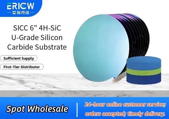
Ultra-high purity (U-Grade) with total metallic impurity concentration < 1 × 10¹⁵ cm⁻³, optimized for high-frequency and high-power device fabrication.
Precision-polished epi-ready surface with RMS roughness ≤ 0.2 nm over full 6-inch diameter, enabling uniform epitaxial growth.
Crystallographically stable 4H polytype with off-axis orientation of 4° toward [11̅20], ensuring step-flow growth mode compatibility.
Low micropipe density (< 0.1 cm⁻²) and negligible basal plane dislocation clusters, supporting high-yield GaN-on-SiC and SiC power device processing.
Thermally robust substrate with excellent dimensional stability up to 1600 °C in inert or vacuum ambient.
High-voltage (>1.2 kV) silicon carbide MOSFETs and Schottky barrier diodes for EV traction inverters and onboard chargers.
RF power amplifiers operating at mmWave frequencies (24–40 GHz) in 5G base station infrastructure.
Heteroepitaxial GaN-on-SiC platforms for high-efficiency power electronics and RF front-end modules.
Radiation-hardened microelectronics for aerospace and satellite power management systems.
High-temperature sensors and MEMS devices requiring stable electrical performance beyond 300 °C.
| Chemical Type | Single-crystal 4H-silicon carbide (SiC) |
| Product Form | Polished wafer, double-side polished (DSP), 6-inch (150 mm) diameter |
| Crystal Orientation | (0001) Si-face, 4° off-axis toward [11̅20] |
| Thickness | 350 ± 10 µm |
| Surface Finish | Epitaxy-ready; Ra ≤ 0.2 nm (AFM, 10 × 10 µm²) |
| Primary Applications | Power electronics, RF devices, high-temperature sensors, heteroepitaxy |
| Key Features | U-Grade purity, low defect density, controlled doping (semi-insulating or N-type optional) |
| Regulatory Compliance | RoHS 2015/863/EU compliant; REACH SVHC-free; no intentional PFAS |
| Common Compatible Systems | Suitability |
| ASM Epsilon® Series CVD Reactors | Highly Recommended – Optimized thermal ramp profiles and SiC-compatible gas chemistry support |
| Aixtron G3™ and G5™ MOCVD Platforms | Highly Recommended – Proven compatibility with 6-inch SiC wafers and GaN/SiC process recipes |
| Applied Materials Centura® Platform (with SiC-optimized chambers) | Recommended – Requires dedicated SiC-compatible hardware and endpoint detection calibration |
| Veeco Nexus® Molecular Beam Epitaxy (MBE) System | Suitable – Validated for low-temperature SiC buffer layer growth under ultra-high vacuum |
Q1: Does SICC 6" 4H-SiC U-Grade have a CAS Registry Number?
A: Yes — CAS No. 409-21-2 applies to crystalline silicon carbide (SiC) as a chemical substance; this identifier covers the bulk material composition of the substrate.
Q2: Is there any risk of elemental leaching or migration from the substrate into epitaxial layers during high-temperature processing?
A: No significant migration occurs under standard epitaxial conditions (≤ 1600 °C, inert/vacuum). U-Grade purity ensures minimal transition metal contamination, and SiC’s covalent lattice structure exhibits negligible elemental diffusion into overgrown GaN or SiC layers.
Q3: How does SICC U-Grade differ from standard A-Grade or B-Grade SiC substrates?
A: U-Grade features stricter impurity control (< 1 × 10¹⁵ cm⁻³ metallic impurities vs. ≥ 1 × 10¹⁶ cm⁻³ for A-Grade), lower micropipe density, tighter thickness uniformity (±10 µm vs. ±25 µm), and enhanced surface planarity—critical for sub-10 nm epitaxial layer control.
Q4: Are certificates of analysis (CoA) and material traceability provided with each wafer shipment?
A: Yes — Each lot includes a full CoA listing individual wafer ID, crystallographic verification (XRD rocking curve FWHM), surface roughness (AFM), resistivity, and impurity screening (GDMS), traceable to ISO/IEC 17025-accredited labs.
Contact With Us:
E-mail: wangxingqiang@ericwchem.com
Have a Questions? Call Us:
Add:
Building A1, Jiete Industrial Park, Huangpu District, Guangzhou City, Guangdong Province, China