English
 Español
 tiếng việt
 русский
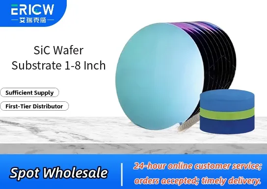
Single-crystal silicon carbide (4H-SiC or 6H-SiC) with low micropipe density (< 0.5 cm⁻²) and high crystalline uniformity.
Available in diameters from 1 inch to 8 inches, supporting scalable device fabrication and process compatibility across R&D and production lines.
Polished double-side wafers (epi-ready) with surface roughness < 0.2 nm RMS and controlled off-axis orientation (4° ± 0.5° toward [11̅20]).
Thermal conductivity > 330 W/m·K at room temperature — enabling superior heat dissipation for high-power electronics.
Chemically inert and oxidation-resistant up to 1600 °C in air — ideal for harsh-environment processing and long-term reliability.
Epitaxial growth platform for high-voltage, high-frequency power devices (e.g., MOSFETs, Schottky diodes, JFETs).
Substrate for RF GaN-on-SiC heterostructures in 5G base station amplifiers and radar systems.
Fabrication of radiation-hardened sensors and detectors for aerospace and nuclear instrumentation.
Platform for wide-bandgap optoelectronic devices including UV photodetectors and deep-UV LEDs.
Research-grade substrate for advanced material studies, including 2D heterostructures and quantum defect engineering.
| Chemical Type | Silicon Carbide (SiC), single-crystal, 4H or 6H polytype |
| Product Form | Polished wafer (double-side polished, epi-ready) |
| Available Diameters | 1 inch, 2 inch, 3 inch, 4 inch, 6 inch, 8 inch |
| Thickness Range | 350 µm – 650 µm (custom thickness available) |
| Surface Finish | Chemomechanical polish (CMP); Ra < 0.2 nm RMS |
| Crystal Orientation | (0001) Si-face, off-axis 4° ± 0.5° toward [11̅20] |
| Primary Applications | Power electronics, RF devices, high-temperature & radiation-hardened electronics |
| Key Features | Low dislocation density, high thermal conductivity, excellent chemical stability |
| Common Compatible Systems | Suitability |
| MOCVD Reactors (e.g., AIXTRON G3, Veeco K465i) | Highly Recommended – Optimized for SiC epitaxy with precise temperature and gas flow control |
| Ion Implantation Systems (e.g., Axcelis GSD, Varian VIISta) | Recommended – Compatible with standard SiC doping profiles and activation annealing |
| Wafer Bonding Platforms (e.g., EVG 850/DBI, SUSS MicroTec XBS300) | Suitable – Supports direct bonding with Si, SiO₂, and metal layers under controlled conditions |
| Atomic Layer Deposition (ALD) Tools (e.g., Beneq TFS 200, Oxford FlexAL) | Recommended – Enables high-quality Al₂O₃, SiO₂, and HfO₂ gate dielectrics on SiC surfaces |
Q1: Does SiC wafer substrate have a CAS Registry Number?
A: No — silicon carbide as a bulk crystalline wafer substrate is not assigned a CAS number; CAS 409-21-2 applies only to silicon carbide powder (non-stoichiometric, amorphous/ceramic grade), not single-crystal semiconductor wafers.
Q2: What is the typical handling protocol to avoid surface contamination or damage during processing?
A: Use Class 100 cleanroom protocols; handle exclusively with PTFE-tipped tweezers and quartz or SiC-compatible carriers; avoid ultrasonic cleaning in organic solvents — prefer RCA-1/RCA-2 followed by HF-last dip for native oxide removal.
Q3: How does SiC compare to sapphire or Si substrates for GaN epitaxy?
A: SiC offers superior lattice match (3.5% mismatch vs. GaN vs. ~13–16% for sapphire/Si), higher thermal conductivity (>3× sapphire, >10× Si), and enables vertical device architectures — resulting in lower on-resistance, higher power density, and improved reliability.
Q4: Are these wafers compliant with RoHS and REACH regulations?
A: Yes — all SiC wafers are manufactured without intentionally added RoHS-restricted substances (Pb, Cd, Hg, Cr⁶⁺, PBB, PBDE) and comply with REACH SVHC thresholds; full compliance documentation available upon request.
Q5: Is there any risk of silicon or carbon migration into epitaxial layers during high-temperature growth?
A: Negligible — single-crystal SiC substrates exhibit exceptional thermal and chemical stability; no measurable Si or C interdiffusion occurs below 1700 °C in standard MOCVD/MBE environments due to strong covalent bonding and low intrinsic diffusion coefficients.
Contact With Us:
E-mail: wangxingqiang@ericwchem.com
Have a Questions? Call Us:
Add:
Building A1, Jiete Industrial Park, Huangpu District, Guangzhou City, Guangdong Province, China