English
 Español
 tiếng việt
 русский
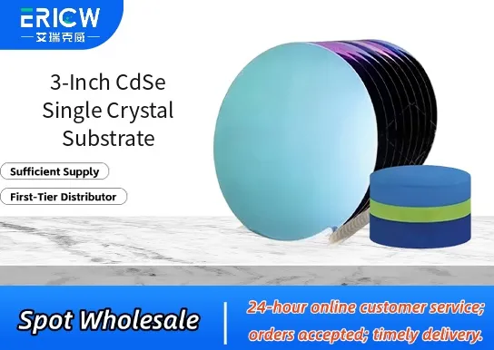
High-purity single-crystal structure with low dislocation density (< 1 × 10⁴ cm⁻²) for superior optoelectronic performance.
Uniform 3-inch (76.2 mm) diameter and ±0.1 mm thickness tolerance, enabling high-yield wafer-level device fabrication.
Chemically stable (0001) basal plane surface, polished to epi-ready finish (Ra < 0.2 nm) with optional Se- or Cd-termination control.
Wide direct bandgap (~1.74 eV at 300 K) ideal for visible-light photodetectors, lasers, and nonlinear optical devices.
Thermally robust up to 720 °C in inert atmosphere, supporting high-temperature MBE and MOCVD epitaxial growth.
Heteroepitaxial growth of II–VI quantum wells and superlattices for tunable visible-light emitters.
Substrate for high-resolution X-ray and electron beam lithography mask blanks in nanofabrication.
Platform for fundamental studies of excitonic physics, valley polarization, and 2D van der Waals heterostructures.
Base material for radiation-hardened photodetectors in space-based optical sensing systems.
Template for seeded crystal growth of CdSe-based nanowires and core–shell nanostructures.
| Chemical Type | Cadmium Selenide (CdSe), ultra-high purity (99.999% min) |
| Product Form | Single-crystal wafer, hexagonal wurtzite structure |
| Orientation | (0001) C-plane, ±0.5° off-axis option available |
| Diameter | 76.2 mm (3.0 inch) ±0.1 mm |
| Thickness | 500 µm ±25 µm (standard); custom thicknesses 350–1000 µm available |
| Surface Finish | Double-side polished; front side epi-ready (Ra < 0.2 nm), back side ground |
| Primary Applications | Epitaxial template, optoelectronic research substrate, calibration standard |
| Regulatory Compliance | RoHS-compliant; REACH SVHC screening performed; SDS available upon request |
| Common Compatible Systems | Suitability |
| Veeco GEN10 MBE System | Highly Recommended – Optimized for CdSe thermal stability and Se-flux control |
| IQE MOCVD Reactor (e.g., CCS-3x2) | Recommended – Compatible with H₂Se and DMCD precursors under standard CdSe growth conditions |
| JEOL JSM-7900F SEM/EBSD Platform | Highly Recommended – Low charging, high crystallographic contrast for orientation mapping |
| Keysight B1500A Semiconductor Parameter Analyzer | Suitable – Supports contact probe testing with standard 3-inch wafer chuck and guard ring configuration |
Q1: What is the CAS Number for CdSe?
A: The CAS Registry Number for cadmium selenide is 1306-23-6.
Q2: Is this substrate suitable for aqueous processing or wet chemical etching?
A: No — CdSe is susceptible to oxidation and dissolution in acidic or oxidizing aqueous environments. Processing requires inert atmosphere, anhydrous solvents, or plasma-based dry etching only.
Q3: How does this CdSe substrate compare to GaAs or Si in terms of lattice matching for epitaxy?
A: CdSe has a lattice constant of a = 4.30 Å, c = 7.01 Å (wurtzite), offering better match to other II–VI compounds (e.g., ZnSe, CdTe) than to III–V or elemental semiconductors. It is not lattice-matched to GaAs (a = 5.65 Å) or Si (a = 5.43 Å), requiring buffer layers or strain-engineered templates.
Q4: Does this product comply with EU SCIP database requirements for articles containing SVHCs?
A: Yes — as a homogeneous material containing cadmium (SVHC candidate), full SCIP submission documentation is provided with commercial orders per Article 9 of EU REACH Regulation (EC) No 1907/2006.
Q5: Can Cd or Se leach into adjacent thin films during high-temperature annealing?
A: Minimal interdiffusion occurs below 550 °C in sealed UHV or high-purity N₂ environments. For temperatures > 550 °C, diffusion barriers (e.g., thin ZnS or AlN capping layers) are recommended to suppress elemental migration.
Contact With Us:
E-mail: wangxingqiang@ericwchem.com
Have a Questions? Call Us:
Add:
Building A1, Jiete Industrial Park, Huangpu District, Guangzhou City, Guangdong Province, China