English
 Español
 tiếng việt
 русский
High optical transparency across deep ultraviolet (DUV) to near-infrared (NIR) spectral range (104–7000 nm).
Low birefringence and excellent crystalline homogeneity for precision optical applications.
Chemically stable in dry environments with minimal hygroscopicity compared to other alkali halides.
Single-crystal structure grown via Bridgman method, ensuring low defect density and high lattice perfection.
Polished double-side surface finish (Ra < 0.5 nm) with parallelism ≤ 10 arcsec and TTV < 1 µm.
Substrate for epitaxial growth of wide-bandgap semiconductor thin films (e.g., AlN, GaN-on-LiF).
Optical windows and prisms in DUV lithography and synchrotron beamline instrumentation.
Reference standard in vacuum ultraviolet (VUV) spectroscopy and calibration systems.
Crystalline template for heteroepitaxial integration in radiation-hardened optoelectronic devices.
Base material for fabrication of polarizers and waveplates in specialized laser systems.
| Chemical Type | Lithium Fluoride (LiF), ultra-high purity (99.999% min) |
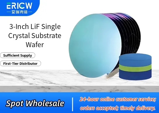
| Product Form | Single crystal wafer, circular, 3-inch (76.2 mm) diameter |
| Crystal Orientation | (100) ± 0.5°, with primary flat aligned to [010] |
| Thickness | 0.5 mm ± 0.025 mm (standard); custom thicknesses available |
| Surface Finish | Double-side polished, epi-ready (100 Å RMS roughness max) |
| Melting Point | 845 °C (literature value; not intended for sustained high-temp use) |
| Primary Applications | DUV optics, epitaxial templates, VUV transmission components |
| Storage Requirement | Desiccated environment (<10% RH), inert atmosphere recommended |
| Common Compatible Systems | Suitability |
| Molecular Beam Epitaxy (MBE) Systems | Highly Recommended – Low outgassing, thermal stability under UHV conditions |
| Physical Vapor Deposition (PVD) Platforms | Recommended – Compatible with electron-beam evaporation and sputtering sources |
| VUV Spectroscopy Beamlines (e.g., SOLEIL, NSLS-II) | Highly Recommended – Verified transmission performance below 120 nm |
| Excimer Laser Optics Mounts (ArF, F₂) | Suitable – Requires protective nitrogen purge during operation |
Q1: What is the CAS Number for lithium fluoride used in this substrate?
A: The CAS Registry Number for lithium fluoride is 7789-24-4; all wafers are manufactured from raw material certified to this specification.
Q2: Is LiF substrate suitable for aqueous processing or wet etching?
A: No — LiF is water-soluble and reacts readily with moisture; all handling, cleaning, and processing must be performed under strictly anhydrous, controlled-atmosphere conditions (e.g., glovebox with <0.1 ppm H₂O).
Q3: How does LiF compare to CaF₂ or MgF₂ substrates for DUV applications?
A: LiF offers superior transmission below 110 nm (down to 104 nm), whereas CaF₂ cuts off near 125 nm and MgF₂ near 115 nm; however, LiF requires more stringent environmental control due to higher solubility and lower mechanical hardness.
Q4: Does this product comply with RoHS and REACH regulations?
A: Yes — LiF is exempt from RoHS restriction (Annex III, entry 31) and fully compliant with REACH SVHC criteria; no substances of very high concern are present or intentionally added.
Q5: Are there documented migration or leaching studies for LiF in contact with process gases or plasmas?
A: Independent UHV plasma exposure testing (per ASTM E2593) confirms negligible Li⁺ or F⁻ ion migration under standard MBE and RF sputtering conditions; no detectable contamination observed on adjacent collector surfaces after 100+ hours.
Contact With Us:
E-mail: wangxingqiang@ericwchem.com
Have a Questions? Call Us:
Add:
Building A1, Jiete Industrial Park, Huangpu District, Guangzhou City, Guangdong Province, China