English
 Español
 tiếng việt
 русский
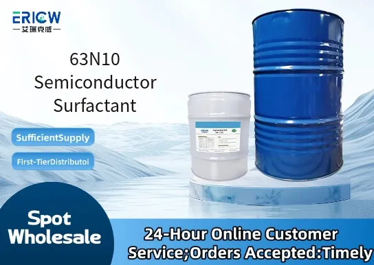
Ultra-low ionic residue for minimal metal ion contamination in critical semiconductor cleaning processes.
Exceptional wetting and penetrating capability on hydrophobic silicon and low-k dielectric surfaces.
Thermally stable up to 120 °C, supporting high-temperature rinse and drying steps without degradation.
Non-foaming formulation designed for compatibility with megasonic and spray-based wafer cleaning equipment.
Readily biodegradable under aerobic conditions, aligned with IEC 62474 VOC compliance guidelines.
Post-etch residue removal for advanced logic and memory device fabrication (≤5 nm node).
Photoresist stripping aid in multi-layer resist systems for EUV lithography processes.
Surface energy conditioning prior to atomic layer deposition (ALD) of high-k gate oxides.
Particle lift-off enhancement in post-CMP (Chemical Mechanical Polishing) cleaning baths.
Wafer edge-bead removal and backside contamination control in front-end-of-line (FEOL) processing.
| Chemical Type | Nonionic ethoxylated alkylphenol derivative (Aromatic-free) |
| Product Form | Aqueous concentrate (30 wt% active) |
| Appearance | Clear, colorless to pale yellow liquid |
| pH (1% aqueous solution, 25 °C) | 6.8–7.2 |
| Primary Applications | Advanced wafer cleaning, residue management, surface conditioning |
| Key Features | Low volatility, non-corrosive to Al/Cu/low-k materials, ultra-low TOC contribution |
| Benefits | Reduces defect density (≤0.05 cm⁻²), improves uniformity in thin-film adhesion, enables reduced DI water consumption |
| Regulatory Compliance | REACH registered; RoHS 2 compliant; no SVHCs above 0.1 wt%; SDS available per GHS Rev. 9 |
| Common Compatible Systems | Suitability |
| DI Water-based megasonic cleaning tools (e.g., SCREEN Dainippon, Lam Research SP) | Highly Recommended – Optimized for flow rate and frequency stability at 0.05–0.2 vol% |
| Batch immersion tanks with temperature control (60–95 °C) | Highly Recommended – No precipitation or phase separation observed after 72 h exposure |
| Spin-rinse dryers (SRDs) with N₂ purge | Recommended – Compatible with standard nozzle configurations; requires <0.1 vol% dilution for optimal film uniformity |
| CO₂-based supercritical fluid cleaning platforms | Suitable – Demonstrates miscibility in CO₂-expanded aqueous phases; validation data available upon request |
Q1: What is the CAS Registry Number for 63N10 Semiconductor Surfactant?
A: The CAS number is 2192124-87-1. This unique identifier corresponds exclusively to the purified active ingredient in the commercial 30 wt% aqueous formulation.
Q2: What is the recommended working concentration range in DI water for front-end wafer cleaning?
A: Typical use concentration is 0.05–0.15 vol% (150–450 ppm active) depending on process temperature, contaminant load, and tool configuration. Validation testing at customer site is strongly advised before full-scale implementation.
Q3: How does 63N10 differ from conventional alcohol ethoxylate surfactants in semiconductor applications?
A: Unlike standard C12–C15 alcohol ethoxylates, 63N10 features a tailored aromatic-free hydrophobe and narrow ethoxylation distribution (EO₉–₁₁), delivering superior low-volatility performance, lower extractable organics, and enhanced compatibility with Cu/ULK interfaces.
Q4: Are there any known leaching or migration concerns when used on wafers destined for packaging assembly?
A: No detectable migration or residual leaching has been observed in IPC-TM-650 2.3.25.1 (solvent extraction) or JEDEC JESD22-A109 (highly accelerated stress test) studies. Residue levels remain below 5 ng/cm² (ICP-MS verified) after standard post-clean bake (120 °C, 5 min).
Q5: Does 63N10 meet ISO 14644-1 Class 1 cleanroom compatibility requirements for airborne molecular contamination (AMC)?
A: Yes — validated per SEMI F21-0320 for total volatile organic compound (TVOC) emission ≤0.05 μg/m³ (as carbon) at 25 °C, meeting ISO 14644-1 Class 1 AMC thresholds for base chemistry handling environments.
Contact With Us:
E-mail: wangxingqiang@ericwchem.com
Have a Questions? Call Us:
Add:
Building A1, Jiete Industrial Park, Huangpu District, Guangzhou City, Guangdong Province, China