English
 Español
 tiếng việt
 русский
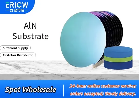
Exceptional thermal conductivity (up to 180–200 W/m·K), enabling efficient heat dissipation in high-power electronic devices.
Wide bandgap (~6.2 eV) and high electrical resistivity (>10¹⁴ Ω·cm), supporting high-voltage and high-frequency operation.
Excellent chemical inertness and resistance to molten metals, halogens, and acidic/alkaline environments at elevated temperatures.
Low dielectric constant (~8.5 at 1 MHz) and minimal dielectric loss (tan δ < 0.001), ideal for RF and microwave substrates.
Thermal expansion coefficient (4.5–5.2 × 10⁻⁶ /K) closely matched to GaN and SiC, reducing interfacial stress during heteroepitaxy.
High-power RF and mmWave semiconductor packaging for 5G base stations and radar systems.
Heteroepitaxial growth platform for GaN-based high-electron-mobility transistors (HEMTs).
Substrate material for deep-ultraviolet (DUV) LEDs and laser diodes (210–280 nm emission range).
Thermal management layers in laser diode arrays and high-brightness LED modules.
Insulating carrier wafers in advanced MEMS and power module assembly processes.
| Chemical Type | Aluminum Nitride (AlN), ultra-high purity (99.99% min) |
| Product Form | Polished single-crystal or high-density polycrystalline wafer/plate |
| Appearance | Off-white to pale yellow, mirror-finish surface (Ra < 0.3 nm on polished side) |
| Melting Point | ~2200 °C (decomposes before melting under ambient pressure) |
| Primary Applications | Power electronics, DUV optoelectronics, RF packaging, thermal interface substrates |
| Key Features | High thermal conductivity, wide bandgap, low CTE, high resistivity, excellent thermal shock resistance |
| Benefits | Enables miniaturization of high-power devices, improves reliability under thermal cycling, supports high-frequency signal integrity |
| Regulatory Compliance | RoHS 2015/863 compliant; REACH SVHC-free; no intentional addition of PFAS or heavy metals |
| Common Compatible Systems | Suitability |
| GaN-on-AlN epitaxy platforms (e.g., MOCVD, HVPE reactors) | Highly Recommended – Minimal lattice mismatch (< 2.5%) and thermal expansion offset enables crack-free heterostructures |
| High-temperature brazing and active metal soldering (e.g., Ag–Cu–Ti alloys) | Highly Recommended – Forms stable interfacial TiN/Al–Ti bonds with excellent shear strength (>120 MPa) |
| Plasma-enhanced CVD (PECVD) and sputtering systems for passivation/metallization | Recommended – Stable under Ar/N₂ plasma; low secondary electron yield minimizes charging effects |
| Wafer-level packaging tools (thermocompression bonders, flip-chip aligners) | Suitable – Rigid mechanical structure and flatness (< 1 µm TTV) ensure precise alignment and uniform bonding pressure |
Q1: What is the CAS Registry Number for aluminum nitride?
A: The CAS Registry Number for aluminum nitride is 24304-00-5.
Q2: Is AlN substrate subject to migration or leaching in humid or aqueous environments?
A: Bulk AlN exhibits negligible hydrolysis below 100 °C and pH 4–10; surface oxidation forms a stable Al₂O₃ layer that further inhibits ion release. No significant Al³⁺ migration is observed per ISO 10993-12 extraction testing (72 h, 50 °C, water/0.9% NaCl).
Q3: How does AlN compare to Al₂O₃ and Si₃N₄ substrates in thermal performance?
A: AlN offers ~10× higher thermal conductivity than standard Al₂O₃ (20–30 W/m·K) and ~2× higher than high-purity Si₃N₄ (90–100 W/m·K), while maintaining comparable mechanical strength and superior electrical insulation.
Q4: Does your AlN substrate carry any food-contact or pharmaceutical regulatory approvals?
A: AlN substrates are not intended for direct food or pharmaceutical contact; they are engineered for industrial electronic and optoelectronic applications. No FDA 21 CFR or EFSA food-contact certification is claimed or applicable.
Contact With Us:
E-mail: wangxingqiang@ericwchem.com
Have a Questions? Call Us:
Add:
Building A1, Jiete Industrial Park, Huangpu District, Guangzhou City, Guangdong Province, China