English
 Español
 tiếng việt
 русский
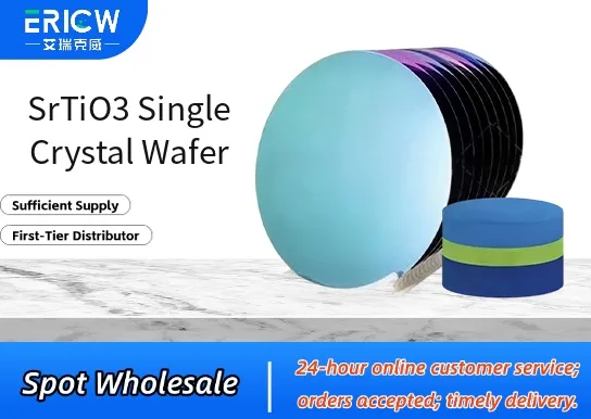
High-purity single-crystal structure with low defect density (dislocation density < 1 × 10⁴ cm⁻²).
Excellent dielectric properties, including high relative permittivity (εᵣ ≈ 300 at 1 kHz) and low dielectric loss (tan δ < 0.001).
Atomically flat surface finish (RMS roughness < 0.2 nm) achieved via mechanical polishing and chemical-mechanical planarization (CMP).
Thermally stable up to 1300 °C in oxidizing atmospheres; retains crystallinity without phase decomposition.
Compatible with standard thin-film deposition techniques including sputtering, PLD, and MBE for heteroepitaxial growth.
Substrate for epitaxial growth of complex oxide thin films (e.g., LaAlO₃, YBCO, LSMO) in quantum materials research.
Active layer or gate dielectric in oxide-based field-effect transistors (OFETs) and memristive devices.
Platform for scanning probe microscopy (SPM) calibration and nanoscale ferroelectric domain studies.
Template for high-temperature superconducting Josephson junction fabrication.
Reference material in X-ray diffraction (XRD), Raman spectroscopy, and ellipsometry metrology standards.
| Chemical Type | Strontium titanate (SrTiO₃), perovskite-structured ceramic |
| Product Form | Polished single-crystal wafer (double-side polished, epi-ready) |
| Crystal Orientation | (001) ± 0.5°, (110) ± 0.5°, or (111) ± 0.5° (customizable) |
| Diameter & Thickness | 10–50 mm diameter; 0.5–1.0 mm thickness (standard: 15 mm × 0.5 mm) |
| Surface Finish | Both sides polished; RMS roughness ≤ 0.2 nm; epi-ready, particle-free |
| Primary Applications | Epitaxial substrate, dielectric platform, quantum device template |
| Key Features | Non-stoichiometric tolerance (Sr/Ti ratio 0.98–1.02), low oxygen vacancy concentration |
| Regulatory Compliance | RoHS-compliant; no REACH SVHC substances above threshold; SDS available upon request |
| Common Compatible Systems | Suitability |
| Pulsed Laser Deposition (PLD) systems (e.g., Newport/Coherent, DCA Instruments) | Highly Recommended – Optimal lattice matching and thermal stability during ablation |
| Molecular Beam Epitaxy (MBE) chambers (e.g., Riber, Veeco) | Highly Recommended – Low outgassing rate and ultra-high vacuum compatibility |
| Sputtering systems (DC/RF magnetron, e.g., Kurt J. Lesker, Angstrom Engineering) | Recommended – Stable under plasma exposure; minimal target poisoning risk |
| Atomic Layer Deposition (ALD) reactors (e.g., Beneq, Oxford Instruments) | Suitable – Surface hydroxyl groups enable uniform nucleation; requires pre-anneal for optimal adhesion |
Q1: What is the CAS Registry Number for SrTiO₃?
A: The CAS Registry Number for strontium titanate (SrTiO₃) is 12060-58-1.
Q2: Is SrTiO₃ wafer suitable for direct contact with food or pharmaceutical products?
A: No — SrTiO₃ wafers are intended for research, semiconductor, and advanced materials applications only; they are not certified for food contact, medical implantation, or pharmaceutical use.
Q3: How does SrTiO₃ compare to MgO or LaAlO₃ as an epitaxial substrate?
A: SrTiO₃ offers superior lattice match for many perovskites (e.g., 0.7% mismatch with YBCO), higher dielectric constant than MgO, and greater thermal/chemical stability than LaAlO₃ under reducing conditions.
Q4: Does SrTiO₃ leach strontium or titanium ions under aqueous or acidic conditions?
A: Bulk SrTiO₃ is highly insoluble in water and mild acids; however, prolonged exposure to strong mineral acids (e.g., >6 M HCl) at elevated temperatures may cause gradual surface dissolution — not recommended for liquid-phase processing without passivation.
Contact With Us:
E-mail: wangxingqiang@ericwchem.com
Have a Questions? Call Us:
Add:
Building A1, Jiete Industrial Park, Huangpu District, Guangzhou City, Guangdong Province, China