English
 Español
 tiếng việt
 русский
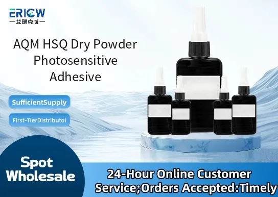
High-resolution patterning capability with sub-micron feature definition under standard UV exposure (i-line, 365 nm).
Thermally stable dry powder form enables long-term shelf life (>24 months at 25 °C, unopened) and eliminates solvent handling risks.
Low outgassing profile suitable for vacuum-based microfabrication processes including MEMS and semiconductor packaging.
Excellent adhesion to silicon, quartz, glass, and metal substrates after thermal cure without primer layers.
Controlled photosensitivity allows precise process window tuning via exposure dose and post-exposure bake (PEB) conditions.
Microlens array fabrication for optical sensors and imaging modules.
Temporary bonding/debonding layers in 3D IC and TSV (through-silicon via) wafer-level packaging.
Maskless lithography resists for rapid prototyping of microfluidic device masters.
Photosensitive dielectric interlayer in flexible hybrid electronics.
High-aspect-ratio photoresist for MEMS structural layer patterning (e.g., accelerometers, gyroscopes).
| Chemical Type | Hydrogen Silsesquioxane (HSQ)-based inorganic-organic hybrid polymer |
| Product Form | Free-flowing white to off-white dry powder |
| Appearance | Uniform fine particulate, particle size distribution D50 ≈ 15–25 µm |
| Primary Applications | Photopatternable temporary adhesive, etch mask, and structural dielectric layer |
| Key Features | Solvent-free, UV-curable, thermally crosslinkable (≥180 °C), high Si–O content |
| Benefits | No VOC emissions, low ash residue (<5% after O₂ plasma ashing), high etch resistance vs. HF-based etchants |
| Regulatory Compliance | REACH SVHC compliant; RoHS 2015/863 Annex II compliant; no listed Prop 65 substances |
| Storage Conditions | 2–8 °C in sealed container under inert gas (N₂); protect from moisture and UV light |
| Common Compatible Systems | Suitability |
| Standard UV Mask Aligners (i-line, 365 nm) | Highly Recommended – Optimized sensitivity and resolution at 100–300 mJ/cm² exposure dose |
| Hot-Press Lamination Equipment (e.g., EVG® 510, Toray TP-500) | Highly Recommended – Uniform film formation achievable at 80–120 °C, 0.5–2 MPa pressure |
| O₂ Plasma Ashing Systems (e.g., March PX-200, Oxford Plasmalab) | Recommended – Complete removal with minimal substrate damage; low carbon residue |
| HF-Based Wet Etch Baths (e.g., 5:1 BHF) | Suitable – Acts as robust etch mask for SiO₂/SiNₓ etching; selectivity >25:1 vs. thermal oxide |
Q1: What is the CAS Registry Number for AQM HSQ Dry Powder Photosensitive Adhesive?
A: The base HSQ polymer component carries CAS No. 17325-27-8; full formulation is proprietary and assigned internal batch-specific documentation per ISO 9001 traceability requirements.
Q2: What is the typical dry-film thickness achieved per gram per square meter (g/m²) during lamination?
A: At standard lamination (100 °C, 1 MPa, 60 s), 1.2–1.5 g/m² yields a uniform 8–12 µm dry film thickness; thickness is adjustable via mass loading and pressure profile.
Q3: How does AQM HSQ compare to traditional PMMA or SU-8 resists in terms of thermal stability and residue after removal?
A: Unlike organic resists, AQM HSQ retains structural integrity up to 400 °C in N₂ and leaves <1% inorganic residue after O₂ plasma ashing—enabling clean interface recovery critical for bonding reuse and multi-layer integration.
Q4: Are there known extractables or leachables under semiconductor-grade cleaning conditions (e.g., SC1, DHF)?
A: No detectable leachables observed under standard wafer cleans (SC1 at 75 °C, 10 min; 0.5% DHF, 25 °C, 60 s) per ICP-MS analysis; fully compatible with front-end-of-line (FEOL) processing environments.
Contact With Us:
E-mail: wangxingqiang@ericwchem.com
Have a Questions? Call Us:
Add:
Building A1, Jiete Industrial Park, Huangpu District, Guangzhou City, Guangdong Province, China