English
 Español
 tiếng việt
 русский
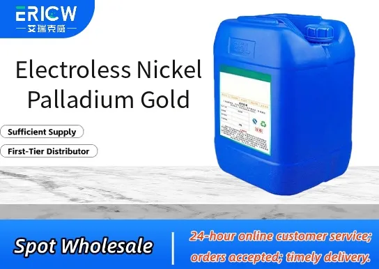
Triple-layer electroless plating system providing exceptional solderability and wire bondability without immersion gold displacement.
Eliminates galvanic corrosion risk between nickel and gold by introducing a diffusion-barrier palladium interlayer.
Superior surface planarity and uniform thickness distribution—even over complex geometries and high-aspect-ratio features.
Lead-free, RoHS-compliant finish compatible with modern halogen-free PCB laminates and assembly processes.
Enhanced oxidation resistance versus conventional electroless nickel immersion gold (ENIG), extending shelf life up to 12 months under controlled storage.
High-reliability printed circuit boards (PCBs) for aerospace and defense avionics systems.
Fine-pitch semiconductor packaging substrates requiring consistent 25–50 µm bond pad definition.
RF/microwave modules where signal integrity demands minimal surface resistivity variation.
Medical electronics assemblies subject to stringent cleanliness and long-term intermetallic stability requirements.
Automotive ADAS control units operating in extended temperature and humidity cycling environments.
| Chemical Type | Autocatalytic ternary alloy deposit (Ni–P–Pd–Au) |
| Product Form | Aqueous multi-bath plating chemistry (separate Ni-P, Pd activation, and Au immersion solutions) |
| Typical Deposit Thickness | Ni-P: 3–6 µm; Pd: 0.05–0.2 µm; Au: 0.03–0.08 µm |
| Appearance | Uniform matte-to-satin yellow metallic finish; non-porous, mirror-smooth under SEM |
| Primary Applications | Surface finish for PCB pads, BGA substrates, RF connectors, and fine-pitch bonding surfaces |
| Key Features | Palladium interlayer inhibits Ni–Au interdiffusion; enables robust thermosonic and ultrasonic wire bonding |
| Benefits | Reduces black pad defects; improves first-pass yield in high-frequency assembly; supports >500 thermal cycles (-55°C to +125°C) |
| Regulatory Compliance | RoHS 2015/863, REACH SVHC-free, IPC-4552B Class 2 certified |
| Common Compatible Systems | Suitability |
| IPC-4552B-compliant ENIG lines with dedicated Pd activation station | Highly Recommended – Designed for seamless integration with existing ENIG infrastructure |
| Vertical continuous plating (VCP) systems with dual-anode configuration | Recommended – Requires minor bath compartment reconfiguration and flow calibration |
| Batch immersion lines with programmable temperature/pH control | Suitable – Validated for low-volume, high-mix production with manual process monitoring |
| Inline spray etch–clean–plate systems with closed-loop filtration | Highly Recommended – Optimized for consistent Pd layer nucleation and Au coverage |
Q1: What is the CAS Registry Number for Electroless Nickel Palladium Gold?
A: Electroless Nickel Palladium Gold is a plated deposit—not a single chemical compound—and therefore has no CAS number. Individual bath components (e.g., nickel sulfate hexahydrate: 10101-97-6; palladium chloride: 7647-10-1; potassium gold cyanide: 13967-50-5) carry distinct CAS identifiers.
Q2: How much gold is consumed per square meter during immersion plating?
A: Typical gold consumption ranges from 0.08–0.12 g/m² for a 0.05 µm nominal deposit, depending on substrate topography, bath age, and immersion time (60–120 seconds at 85–90°C).
Q3: How does ENPG compare to ENEPIG and standard ENIG in terms of intermetallic growth control?
A: ENPG’s palladium interlayer significantly suppresses Ni₃Sn₄ formation during soldering and aging—outperforming ENIG (no barrier) and matching ENEPIG in thermal stability, while offering superior Au adhesion and lower cost than full ENEPIG stacks.
Q4: Are there known migration or leaching concerns under humid bias testing?
A: Independent IPC TM-650 2.6.25 testing shows no measurable ionic migration or gold leaching after 1000 hours at 85°C/85% RH with 5 V bias—attributable to the dense, low-porosity Pd barrier layer.
Q5: Does ENPG meet IPC-4556 for high-frequency applications?
A: Yes—ENPG deposits meet IPC-4556 Class A requirements for insertion loss, return loss, and surface roughness (Ra < 0.05 µm), making them qualified for mmWave (24–77 GHz) antenna-in-package and 5G baseband substrates.
Contact With Us:
E-mail: wangxingqiang@ericwchem.com
Have a Questions? Call Us:
Add:
Building A1, Jiete Industrial Park, Huangpu District, Guangzhou City, Guangdong Province, China