English
 Español
 tiếng việt
 русский
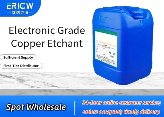
Ultra-low metallic impurity profile (<10 ppt Na, K, Fe, Ni, Cr, and Zn) ensuring minimal device contamination.
Controlled etch rate uniformity (±3% across 300 mm wafers) for high-precision pattern transfer.
Non-oxidizing, chloride-free formulation to prevent copper redeposition and micro-roughening.
pH-stabilized aqueous solution with built-in corrosion inhibitors for extended bath life (>120 hours at 45°C).
Compatible with standard photoresist stripping and post-etch cleaning processes without residue formation.
Front-end-of-line (FEOL) copper interconnect patterning in advanced logic and memory IC fabrication (≤7 nm nodes).
Microvia etching for high-density interconnect (HDI) PCBs and embedded substrate applications.
Thin-film copper removal in MEMS and RF filter manufacturing.
Back-end-of-line (BEOL) redistribution layer (RDL) definition for fan-out wafer-level packaging (FOWLP).
Research & development of Cu-based transparent conductive films and flexible hybrid electronics.
| Chemical Type | Aqueous ammoniacal complex etchant (non-acidic, non-halogenated) |
| Product Form | Liquid concentrate (ready-to-dilute) |
| Appearance | Clear, pale blue solution, free of particulates or haze |
| Primary Applications | Wet etching of electroplated and sputtered copper films (20–500 nm thickness) |
| Key Features | Low total organic carbon (TOC < 50 ppb), ultra-high purity packaging (Class 1 cleanroom filled) |
| Benefits | Reduced defect density, improved CD control, no undercut beyond specification (≤0.1 µm @ 0.3 µm line) |
| Regulatory Compliance | REACH SVHC-free, RoHS 3 compliant, TSCA-listed, ISO 9001 & ISO 14001 certified manufacturing |
| Storage Stability | 24 months unopened at 15–25°C; protected from light and moisture |
| Common Compatible Systems | Suitability |
| SEZ® Spin Rinse Dryer (SRD) platforms | Highly Recommended – Optimized for single-wafer processing with integrated temperature and flow control |
| Screen® Semiconductor Wet Processing Tools | Recommended – Requires minor nozzle calibration for uniform spray distribution |
| Modutek® Teflon®-lined batch immersion tanks | Suitable – Compatible with PFA and quartz wet benches; use with recirculating filtration (0.1 µm) |
| Applied Materials® Eterna™ CPM systems | Highly Recommended – Validated for multi-layer Cu/Ta/N barrier stack etching with inline metrology integration |
Q1: What is the CAS Registry Number for this electronic grade copper etchant?
A: This product is a proprietary multi-component formulation and does not have a single CAS number; individual high-purity components are documented in the Safety Data Sheet (SDS) Section 3.
Q2: What is the recommended working concentration and typical etch rate at 40°C?
A: Dilute 1:4 (v/v) with deionized water (18.2 MΩ·cm); typical etch rate is 120–140 Å/sec on 200 nm electroplated Cu at 40 ± 0.5°C with agitation.
Q3: How does this etchant compare to traditional ferric chloride or ammonium persulfate solutions?
A: Unlike aggressive oxidizers, this etchant provides isotropic but highly controllable removal with negligible attack on TaN/Ta barriers, no chlorine-induced corrosion, and >99.9% copper ion recovery compatibility via electrowinning.
Q4: Does it meet semiconductor industry migration testing requirements (e.g., JEDEC JESD22-A106 for ionic leachables)?
A: Yes — validated per JEDEC JESD22-A106B (96-hour 85°C/85% RH) showing Na⁺, Cl⁻, and NH₄⁺ extractables < 5 ng/cm² on bare silicon wafers.
Q5: Is there any risk of copper re-deposition or particle generation during extended bath use?
A: No — the chelating stabilizer system prevents Cu⁰ nucleation; validated by SEM/EDS analysis after 100 hours of continuous operation shows zero detectable redeposited copper particles (>0.1 µm).
Contact With Us:
E-mail: wangxingqiang@ericwchem.com
Have a Questions? Call Us:
Add:
Building A1, Jiete Industrial Park, Huangpu District, Guangzhou City, Guangdong Province, China