English
 Español
 tiếng việt
 русский
High-resolution negative-tone imaging capability with sub-10 nm feature definition in e-beam lithography.
Excellent thermal stability up to 1000 °C in inert atmospheres, enabling high-temperature etch and release processes.
Low outgassing profile suitable for vacuum-compatible MEMS and nanofabrication environments.
Water-developable formulation eliminates need for organic solvents, enhancing workplace safety and environmental compliance.
Consistent 22 wt% solid content ensures reproducible film thickness control across spin-coating processes (e.g., 100–300 nm at 3000–5000 rpm).
Nanoscale mask fabrication for extreme ultraviolet (EUV) and electron-beam lithography.
High-aspect-ratio nanostructure patterning in silicon carbide (SiC), gallium nitride (GaN), and quartz substrates.
Release layer and sacrificial template in MEMS/NEMS device fabrication and nanoimprint stamping.
Direct-write nanolithography for quantum device prototyping and plasmonic metasurface fabrication.
Hard mask application in deep reactive ion etching (DRIE) of silicon and compound semiconductors.
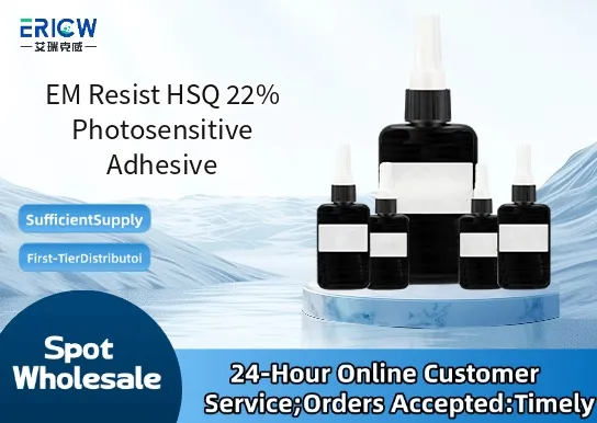
| Chemical Type | Hydrogen Silsesquioxane (HSQ) based negative-tone photoresist |
| Product Form | Liquid solution in methyl isobutyl ketone (MIBK) |
| Appearance | Clear, colorless to pale yellow liquid |
| Solid Content | 22 ± 0.5 wt% |
| Viscosity (25 °C) | 4.5–5.5 cP |
| Primary Applications | E-beam lithography, high-resolution hard mask, nanoscale templating |
| Key Features | Electron-sensitive, inorganic silica network after curing, high etch resistance |
| Regulatory Compliance | REACH compliant; RoHS 2015/863 Annex II compliant; no SVHCs above threshold |
| Common Compatible Systems | Suitability |
| JEOL JSM & JEM series e-beam writers (e.g., JSM-7900F, JEM-ARM300F) | Highly Recommended – Optimized sensitivity at 100 keV; validated dose range: 100–1000 μC/cm² |
| Canon FPA-1200NZ2C (EUV scanner with resist underlayer) | Recommended – Requires HMDS priming and optimized PAB/PEB; used as EUV hard mask stack component |
| Spin coaters (Laurell WS-650, Headway EC301) | Highly Recommended – Compatible with standard 4″–8″ wafer chucks and MIBK-wet cleaning protocols |
| Plasma etch systems (Oxford Instruments ICP-RIE, STS Multiplex) | Highly Recommended – Demonstrates >15:1 selectivity over Si in SF₆/O₂ chemistries |
Q1: What is the CAS Number for EM Resist HSQ 22%?
A: The base HSQ polymer component has CAS No. 33999-44-7; the full formulated product (including MIBK solvent) is assigned proprietary batch-specific registration per REACH Annex VI requirements.
Q2: What is the recommended spin-coating speed and post-apply bake (PAB) condition?
A: For 200 nm nominal thickness on Si wafers: spin at 4000 rpm for 30 s; PAB at 90 °C for 90 s on a hotplate with nitrogen purge. Avoid prolonged ambient exposure pre-bake to prevent moisture uptake.
Q3: How does EM Resist HSQ 22% compare to XR-1541 or Dow Corning® HSQ-26?
A: EM Resist HSQ 22% offers tighter molecular weight distribution and lower metal ion contamination (<1 ppb Na/K/Ca) than legacy HSQ formulations, resulting in improved pattern fidelity and reduced defect density in <20 nm features.
Q4: Is extraction or migration of components into process fluids a concern during wet development?
A: No measurable leaching occurs during standard deionized water development (2 min agitation, 23 °C). Residual organics are fully removed in the initial rinse; cured HSQ forms an inert, non-soluble silica network.
Contact With Us:
E-mail: wangxingqiang@ericwchem.com
Have a Questions? Call Us:
Add:
Building A1, Jiete Industrial Park, Huangpu District, Guangzhou City, Guangdong Province, China