English
 Español
 tiếng việt
 русский
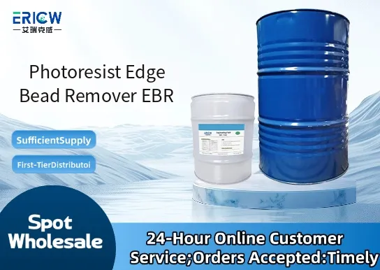
Highly selective removal of photoresist edge beads without undercutting or damaging underlying resist patterns.
Low surface tension formulation ensures uniform coverage and effective capillary action at wafer edges.
Non-corrosive to aluminum, copper, titanium, and low-k dielectric materials commonly used in advanced semiconductor processes.
Fast-evaporating solvent blend enables rapid processing and minimal dwell time on wafers.
Compatible with both positive and negative tone photoresists across g-line, i-line, KrF, and ArF lithography platforms.
Semiconductor front-end-of-line (FEOL) and back-end-of-line (BEOL) photolithography process steps.
Advanced packaging applications including fan-out wafer-level packaging (FOWLP) and 2.5D/3D integration.
MEMS and sensor fabrication requiring precise edge definition and residue-free sidewalls.
Compound semiconductor manufacturing for GaAs, SiC, and GaN-based devices.
Display panel production using thin-film transistor (TFT) patterning on glass and flexible substrates.
| Chemical Type | Proprietary solvent blend (non-halogenated) |
| Product Form | Liquid (ready-to-use) |
| Appearance | Clear, colorless liquid |
| Boiling Point Range | 85–110 °C |
| Primary Applications | Edge bead removal after spin-coating of photoresist |
| Key Features | Resist-selective, low particulate, ultra-low metal ion content (<1 ppb) |
| Benefits | Reduces post-litho defects, improves CD uniformity, enhances yield in high-volume manufacturing |
| Regulatory Compliance | REACH compliant; RoHS 2015/863 Annex II compliant; no SVHCs above threshold |
| Common Compatible Systems | Suitability |
| TOKYO ELECTRON (TEL) CLEAN TRACK™ series | Highly Recommended – Optimized dispensing and rinse protocols validated |
| SCREEN Semiconductor Solutions Dainippon Screen MZ series | Highly Recommended – Fully integrated into edge bead removal modules |
| DISCO DFP8760 / DFP8860 Edge Trim Systems | Recommended – Requires minor nozzle calibration for optimal coverage |
| Manual spin coater + edge rinse station (e.g., Laurell WS-650) | Suitable – Compatible with standard syringe or spray-based manual application |
Q1: What is the CAS Registry Number for Photoresist Edge Bead Remover EBR?
A: This is a proprietary multi-component formulation; individual components are disclosed under NDA, and no single CAS number applies to the finished product. Full ingredient disclosure is available upon execution of a CDA.
Q2: What is the recommended dosage per 200 mm wafer?
A: Typical usage is 0.8–1.2 mL per 200 mm wafer, applied via precision dispense nozzle during edge rinse step; volume may vary based on resist thickness and spin speed.
Q3: How does EBR compare to acetone or IPA for edge bead removal?
A: Unlike acetone or IPA, EBR offers superior selectivity, reduced resist swelling, and no adverse interaction with anti-reflective coatings (BARC) or adhesion promoters—critical for sub-28 nm node processes.
Q4: Is EBR certified for use in ISO Class 1 cleanrooms?
A: Yes—manufactured and packaged in ISO Class 3 (Class 1 at point-of-use) cleanroom environments; certified for particle count <1 particle/mL @ ≥0.2 µm (per JIS B 9921).
Q5: Has extractable/leachable testing been performed for high-aspect-ratio via applications?
A: Yes—validated per USP <87> and <88>; no detectable leachables (<0.1 ppm) observed in post-rinse analysis for Cu, Co, Ta, and SiO₂ surfaces after 60 s exposure at 23 °C.
Contact With Us:
E-mail: wangxingqiang@ericwchem.com
Have a Questions? Call Us:
Add:
Building A1, Jiete Industrial Park, Huangpu District, Guangzhou City, Guangdong Province, China