English
 Español
 tiếng việt
 русский
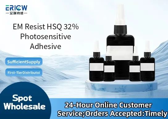
High-resolution negative-tone imaging capability with sub-10 nm feature definition in e-beam lithography.
Excellent thermal stability up to 1000 °C in inert atmospheres, enabling high-temperature annealing and etch processes.
Low outgassing profile suitable for ultra-high vacuum (UHV) and electron-beam lithography systems.
Spin-coatable formulation with consistent film uniformity and controllable thickness (50–500 nm typical).
Hydrogen silsesquioxane (HSQ)-based chemistry offering inherent inorganic character post-development and curing.
Nanofabrication of quantum devices, including single-electron transistors and superconducting qubits.
Maskless lithography for research and prototyping in semiconductor R&D laboratories.
Hard mask formation for high-aspect-ratio silicon etching in MEMS and nanoelectromechanical systems.
Direct-write patterning of plasmonic nanostructures and photonic crystal templates.
Fabrication of nanoscale X-ray and EUV mask absorber layers.
| Chemical Type | Hydrogen silsesquioxane (HSQ) oligomer solution |
| Product Form | Clear, colorless liquid (32 wt% solids in methyl isobutyl ketone, MIBK) |
| Appearance | Transparent, low-viscosity solution; slight opalescence permissible |
| Primary Applications | E-beam lithography, direct-write nanofabrication, hard mask patterning |
| Key Features | Electron-sensitive, inorganic network after curing, high etch resistance |
| Benefits | Sub-10 nm resolution, minimal line-edge roughness (LER), no carbon residue post-etch |
| Storage Conditions | 4 °C, under nitrogen, protected from light and moisture |
| Shelf Life | 12 months from date of manufacture when stored properly |
| Common Compatible Systems | Suitability |
| JEOL JSM/JSW series e-beam lithography tools | Highly Recommended – Optimized exposure dose and development protocols available |
| RAITH eLINE / VOYAGER platforms | Highly Recommended – Pre-validated process recipes included in support package |
| Hitachi SU9000 / S-4800 SEM-based lithography setups | Recommended – Requires minor focus/dose calibration for optimal contrast |
| Standard spin coaters (e.g., Laurell WS-650MZ-23NPP) | Suitable – Compatible with standard 100–4000 rpm spin profiles and soft bake steps |
| TMAH-based developers (2.38% aqueous tetramethylammonium hydroxide) | Suitable – Industry-standard developer; recommended for high-fidelity pattern transfer |
Q1: What is the CAS Registry Number for EM Resist HSQ 32%?
A: The base HSQ polymer component is assigned CAS No. 17378-61-3; the full formulated product (32% in MIBK) does not have a unique CAS number per regulatory convention for solvent-based mixtures.
Q2: What is the recommended spin speed range to achieve a 100 nm film thickness?
A: For 100 nm nominal thickness on silicon wafers, spin at 3000–3500 rpm for 30 seconds; exact speed depends on substrate geometry, temperature, and ambient humidity — process optimization is advised for critical applications.
Q3: How does EM Resist HSQ 32% compare to XR-1541 or FOXP-16 in terms of resolution and etch resistance?
A: EM Resist HSQ offers superior resolution (<10 nm vs. ~20 nm for XR-1541) and significantly higher silicon etch resistance than organic resists like FOXP-16 due to its inorganic SiO₂-like network after curing.
Q4: Is EM Resist HSQ 32% compliant with REACH and RoHS directives?
A: Yes — all components comply with current REACH SVHC and RoHS 2 (2015/863/EU) requirements; SDS and regulatory documentation are available upon request.
Q5: Are there known migration or extractable concerns when used in proximity to sensitive analytical surfaces (e.g., TEM grids or mass spectrometry sources)?
A: When fully cured (≥800 °C in N₂), HSQ forms a stable, non-volatile silica network with negligible outgassing or leaching; residual uncured material must be removed via O₂ plasma or wet development prior to high-vacuum use.
Contact With Us:
E-mail: wangxingqiang@ericwchem.com
Have a Questions? Call Us:
Add:
Building A1, Jiete Industrial Park, Huangpu District, Guangzhou City, Guangdong Province, China