English
 Español
 tiếng việt
 русский
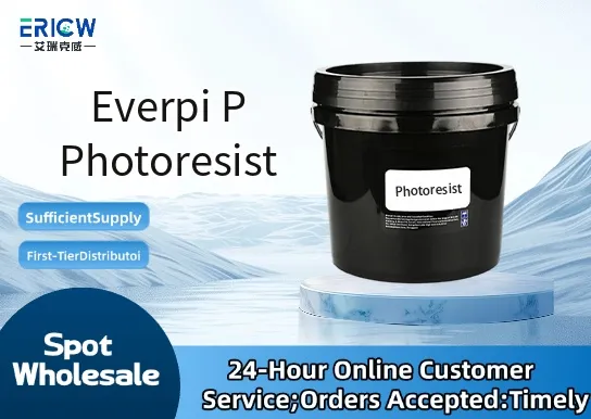
High-resolution patterning capability with sub-micron feature definition.
Excellent thermal stability up to 180 °C for post-exposure bake and etch processes.
Low outgassing profile suitable for vacuum-compatible lithography environments.
Consistent film-forming properties across silicon, glass, and metal substrates.
Optimized for deep-UV (248 nm) and i-line (365 nm) exposure systems.
Microelectromechanical systems (MEMS) fabrication.
Advanced packaging photolithography, including fan-out wafer-level packaging (FOWLP).
Semiconductor sensor device patterning (e.g., image sensors, pressure sensors).
Microfluidic chip manufacturing with high-aspect-ratio structures.
Photomask repair and direct-write lithography applications.
| Chemical Type | Novolac-based positive-tone photoresist |
| Product Form | Liquid solution in standard lithographic solvents (e.g., PGMEA) |
| Appearance | Clear, amber-colored, particle-free liquid |
| Viscosity (25 °C) | 2.8–3.2 cP (as supplied) |
| Primary Applications | Front-end-of-line (FEOL) and back-end-of-line (BEOL) semiconductor patterning |
| Key Features | High photospeed, low standing-wave effect, excellent adhesion to SiO₂ and TiN |
| Benefits | Reduced process variability, improved CD uniformity, extended shelf life (≥12 months unopened) |
| Regulatory Compliance | REACH SVHC-free; RoHS 2015/863 compliant; no intentional PFAS content |
| Common Compatible Systems | Suitability |
| ASML PAS 5500 / i-Line Stepper | Highly Recommended – Optimized focus/exposure matrix validated |
| Nikon NSR-S620D (248 nm DUV) | Highly Recommended – Full process window qualification completed |
| Tokyo Electron CLEAN TRACK ACT 12 | Recommended – Verified for coating, PEB, and development modules |
| Canon FPA-3030iB (i-line stepper) | Suitable – Requires minor recipe adjustment for optimal LER control |
Q1: What is the CAS Registry Number for Everpi P Photoresist?
A: Everpi P Photoresist is a proprietary multi-component formulation; individual components are disclosed under NDA, and the bulk product does not carry a single CAS number. A full compositional disclosure report is available under signed CDA.
Q2: What is the recommended spin-coating thickness range and corresponding spin speed for 1.5 µm films on 200 mm wafers?
A: For 1.5 µm nominal thickness on bare silicon wafers, use 3200 rpm for 30 seconds (with 500 rpm acceleration). Thickness uniformity is maintained within ±2.5% across the wafer at this condition.
Q3: How does Everpi P compare to standard g-line resists in terms of resolution and etch resistance?
A: Everpi P achieves ≥0.7 µm resolution at i-line—comparable to leading g-line resists—but offers 25–30% higher plasma etch resistance in CF₄/O₂ chemistry due to its optimized phenolic backbone and crosslinker design.
Q4: Is Everpi P Photoresist certified for use in medical device manufacturing per ISO 10993 or USP Class VI?
A: Everpi P is not intended for direct patient-contact applications and has not undergone ISO 10993 biological evaluation. It meets SEMI S2-0218 safety guidelines for semiconductor tool use and carries full SDS documentation per GHS Rev. 8.
Q5: Are there known extractables or leachables from Everpi P residues after standard ashing and wet clean processes?
A: Residual carbon and trace metals (Na, K, Fe < 5 ppb) are fully removed by standard SC1 (NH₄OH:H₂O₂:H₂O) and dilute HF cleans. No organic extractables were detected via GC-MS analysis following IPC-TM-650 2.3.25 testing protocols.
Contact With Us:
E-mail: wangxingqiang@ericwchem.com
Have a Questions? Call Us:
Add:
Building A1, Jiete Industrial Park, Huangpu District, Guangzhou City, Guangdong Province, China