English
 Español
 tiếng việt
 русский
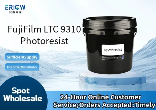
High-resolution patterning capability for sub-micron lithography processes.
Excellent thermal stability and post-exposure bake (PEB) latitude for robust process control.
Superior adhesion to silicon, silicon dioxide, and metal substrates without additional primers.
Low outgassing profile compatible with vacuum-based exposure tools including EUV and DUV steppers.
Optimized for high-throughput manufacturing with consistent film uniformity and minimal defect generation.
Advanced semiconductor front-end-of-line (FEOL) interconnect patterning.
MEMS and microfluidic device fabrication requiring precise topography control.
Power device manufacturing, including IGBT and SiC MOSFET gate patterning.
Compound semiconductor processing for GaN and GaAs RF devices.
Advanced packaging applications such as redistribution layer (RDL) and via-first fan-out wafer-level packaging (FO-WLP).
| Chemical Type | Positive-tone, chemically amplified resist (CAR) |
| Product Form | Liquid solution in proprietary solvent blend |
| Appearance | Clear, pale yellow liquid |
| Primary Applications | Deep UV (248 nm) and immersion lithography (193 nm) |
| Key Features | High sensitivity (~15 mJ/cm² at 193 nm), low LWR (<3.0 nm), high etch resistance |
| Benefits | Reduced cycle time, improved CD uniformity, compatibility with multi-patterning schemes |
| Regulatory Compliance | REACH SVHC-free; RoHS 3 compliant; no intentionally added PFAS |
| Storage Conditions | 2–8 °C in sealed container; protect from light and moisture |
| Common Compatible Systems | Suitability |
| Nikon NSR-S630D Stepper | Highly Recommended – Validated for full-field exposure with standard illumination conditions |
| ASML NXT:1980Di Immersion Scanner | Highly Recommended – Qualified for 193i lithography with optimized dose and focus settings |
| TOK Coater/Developer System (CLEAN TRACK LITHIUS Pro Z) | Recommended – Requires minor process recipe adjustment for optimal develop uniformity |
| Screen Semiconductor Coater/Developer (SD-1000 Series) | Suitable – Functional with standard pre-bake and development parameters; verification recommended per tool configuration |
Q1: What is the CAS Registry Number for FujiFilm LTC 9310 Photoresist?
A: FujiFilm LTC 9310 is a proprietary multi-component formulation; individual CAS numbers are not assigned to the final product. Component-specific CAS numbers are available under NDA upon request from Fujifilm Business Innovation Corp.
Q2: What is the typical spin-coating thickness range and corresponding recommended spin speed?
A: Achieves 100–300 nm dry film thickness at 1500–3500 rpm (depending on substrate and desired resolution); optimal performance observed at 2200 rpm for 200 nm nominal thickness on bare silicon wafers.
Q3: How does LTC 9310 compare to Fujifilm’s older LTC 7000 series in terms of sensitivity and LER performance?
A: LTC 9310 offers ~35% higher sensitivity and ~40% lower line edge roughness (LER) versus LTC 7000 under identical 193i process conditions, enabled by next-generation PAG and polymer design.
Q4: Is LTC 9310 compliant with ISO 10993 or USP Class VI for medical device lithography applications?
A: LTC 9310 is not certified to ISO 10993 or USP Class VI, as it is formulated for semiconductor-grade use only. Residual monomer and extractables are minimized per SEMI standards, but biocompatibility testing is not performed.
Q5: Are there documented migration or leaching studies for LTC 9310 in contact with aqueous or acidic environments after development?
A: No migration or leaching data exists for developed LTC 9310 films in aqueous environments, as the material is designed for permanent integration into semiconductor structures and is removed entirely during subsequent etch or ash steps.
Contact With Us:
E-mail: wangxingqiang@ericwchem.com
Have a Questions? Call Us:
Add:
Building A1, Jiete Industrial Park, Huangpu District, Guangzhou City, Guangdong Province, China