English
 Español
 tiếng việt
 русский
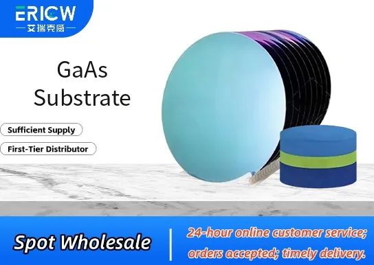
Single-crystal gallium arsenide wafer with high structural uniformity and low dislocation density (< 1 × 10⁴ cm⁻²).
Excellent electron mobility (≈8500 cm²/V·s at 300 K) enabling high-frequency device performance.
Direct bandgap of 1.42 eV at room temperature, ideal for optoelectronic integration.
Chemically stable under standard cleanroom processing conditions (e.g., HCl, NH₄OH, H₂O₂).
Available in polished, etch-polished, or epitaxial-ready surface finishes with controlled off-cut angles (e.g., 2° toward [110]).
Epitaxial growth platform for high-electron-mobility transistors (HEMTs) and heterojunction bipolar transistors (HBTs).
Fabrication of infrared light-emitting diodes (LEDs), laser diodes (LDs), and photodetectors operating in 700–900 nm range.
Substrate for monolithic microwave integrated circuits (MMICs) used in 5G infrastructure and radar systems.
Base material for space-qualified solar cells due to radiation hardness and high power conversion efficiency (>28% under AM0).
Platform for quantum well and quantum dot nanostructure research in solid-state physics laboratories.
| Chemical Type | Gallium Arsenide (GaAs), semi-insulating or n-type doped |
| Product Form | Polished single-crystal wafer (standard diameters: 2", 3", 4", 6") |
| Crystal Orientation | (100) ± 0.5°, with optional (111)A/B orientations |
| Surface Finish | Double-side polished (DSP), EPI-ready, or etch-polished; RMS roughness < 0.3 nm |
| Melting Point | 1238 °C (decomposes before melting under ambient pressure) |
| Primary Applications | RF/microwave devices, optoelectronics, photovoltaics, quantum research |
| Key Features | High resistivity (>1 × 10⁷ Ω·cm for SI grade), low oxygen/carbon contamination |
| Regulatory Compliance | RoHS-compliant; no intentionally added REACH SVHC substances |
| Common Compatible Systems | Suitability |
| MOCVD (Metalorganic Chemical Vapor Deposition) | Highly Recommended – Optimized for GaAs-based epitaxy (e.g., AlGaAs, InGaP) |
| MBE (Molecular Beam Epitaxy) | Highly Recommended – Ultra-high vacuum compatibility and precise layer control |
| Photolithography & Wet Etching Stations (e.g., HCl/H₃PO₄-based) | Recommended – Stable against common semiconductor etchants |
| Ion Implantation Systems | Suitable – Acceptable channeling behavior and damage recovery post-anneal |
Q1: What is the CAS Registry Number for GaAs substrate material?
A: The CAS number for gallium arsenide is 1303-00-0.
Q2: Is GaAs substrate suitable for direct contact with food, pharmaceuticals, or drinking water?
A: No — GaAs substrates are not intended for consumer-end contact applications. They are strictly for semiconductor fabrication and R&D use under controlled industrial environments.
Q3: How does GaAs compare to silicon (Si) and silicon carbide (SiC) substrates in high-power RF applications?
A: GaAs offers superior electron mobility and semi-insulating properties vs. Si, enabling lower noise and higher frequency operation (up to 100+ GHz), but lower thermal conductivity than SiC — making SiC preferable for ultra-high-power density applications.
Q4: Are there documented migration or leaching studies for GaAs under semiconductor processing conditions?
A: Yes — trace arsenic release is tightly controlled per SEMI F57 standards; wafers meet ITRS specifications for surface metallic contamination (< 1 × 10¹⁰ atoms/cm² for As, Ga, and transition metals after SC1 clean).
Contact With Us:
E-mail: wangxingqiang@ericwchem.com
Have a Questions? Call Us:
Add:
Building A1, Jiete Industrial Park, Huangpu District, Guangzhou City, Guangdong Province, China