English
 Español
 tiếng việt
 русский
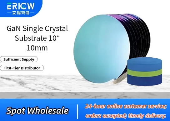
Ultra-low dislocation density (< 1 × 10⁶ cm⁻²) enabling high-efficiency optoelectronic and power device fabrication.
High thermal conductivity (~230 W/m·K) for superior heat dissipation in high-power RF and laser applications.
Chemically stable single-crystal structure with minimal lattice mismatch to epitaxial GaN layers.
Optimized surface finish (Ra < 0.2 nm) achieved via mechanical polishing and chemical-mechanical planarization (CMP).
Available with customizable orientations (c-plane, m-plane, semi-polar) and optional backside metallization or SiO₂ passivation.
High-brightness blue/UV LEDs and laser diodes requiring low-defect templates for high quantum efficiency.
Next-generation GaN-on-GaN power transistors for 5G base stations and EV inverters.
High-frequency millimeter-wave (mmWave) RF amplifiers operating above 30 GHz.
Deep-UV photodetectors and solid-state lighting systems demanding high crystalline integrity.
Research platforms for heteroepitaxial growth of AlGaN, InGaN, and hybrid perovskite/GaN heterostructures.
| Chemical Type | Gallium Nitride (GaN), single crystal |
| Product Form | Free-standing wafer substrate |
| Dimensions | 10.0 mm × 10.0 mm × 350 ± 25 µm (standard thickness) |
| Crystal Orientation | c-plane (0001), with optional m-plane (1-100) or r-plane (1-102) |
| Surface Finish | Double-side polished; front: epi-ready CMP; back: mechanical polish |
| Primary Applications | Epitaxial growth template for GaN-based devices |
| Key Features | Low threading dislocation density, high thermal stability (>1000 °C in N₂), negligible wafer bow (< 5 µm) |
| Regulatory Compliance | RoHS 2015/863/EU compliant; REACH SVHC-free; no conflict minerals used |
| Common Compatible Systems | Suitability |
| MOCVD Reactors (e.g., AIXTRON G3, Veeco K465i) | Highly Recommended – Optimized for uniform GaN nucleation and low-temperature buffer layer growth |
| MBE Systems (e.g., Riber Crea, SVT Associates) | Recommended – Compatible with nitrogen plasma sources and Ga effusion cells |
| Atomic Layer Deposition (ALD) Platforms (e.g., Beneq TFS 200) | Suitable – Supports uniform Al₂O₃ or SiO₂ passivation without substrate degradation |
| Laser Lift-Off (LLO) and Wafer Bonding Tools | Highly Recommended – Minimal thermal stress during UV excimer laser processing (248 nm) |
Q1: Does GaN single crystal substrate have a CAS Registry Number?
A: Yes — Gallium nitride has CAS No. 25617-97-4; however, this number applies to bulk GaN compound, not the engineered single-crystal substrate. The substrate itself is classified as a manufactured article under REACH and is exempt from CAS-based substance registration.
Q2: What is the recommended handling protocol to avoid surface contamination or oxidation?
A: Store in Class 100 cleanroom conditions under dry N₂ atmosphere; handle only with quartz or PTFE-tipped tweezers; clean using sequential acetone/isopropanol ultrasonication followed by N₂ blow-dry — avoid aqueous HF or strong acids that may etch Ga-terminated surfaces.
Q3: How does GaN-on-GaN compare to GaN-on-SiC or GaN-on-sapphire in terms of thermal management and defect density?
A: GaN-on-GaN eliminates lattice and thermal expansion mismatch, reducing dislocation density by >3 orders of magnitude versus sapphire and improving thermal conductivity by ~40% versus SiC. This enables higher power density and longer device lifetime under continuous operation.
Q4: Are there any known leaching or ion migration concerns when used in contact with process chemicals or under bias?
A: GaN single crystal substrates exhibit negligible Ga³⁺ or N³⁻ ion migration under standard semiconductor processing conditions (pH 2–12, < 200 °C). No measurable metal ion extraction occurs in DI water or dilute HCl (0.1 M) after 72 h immersion per ASTM F2129 corrosion testing.
Contact With Us:
E-mail: wangxingqiang@ericwchem.com
Have a Questions? Call Us:
Add:
Building A1, Jiete Industrial Park, Huangpu District, Guangzhou City, Guangdong Province, China