English
 Español
 tiếng việt
 русский
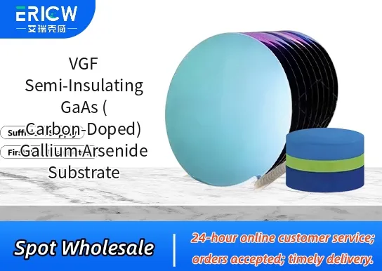
Ultra-high resistivity (>1 × 10⁸ Ω·cm at 300 K) achieved via controlled carbon doping in the vertical gradient freeze (VGF) crystal growth process.
Exceptional crystalline quality with low dislocation density (<5 × 10³ cm⁻²), enabling high-yield epitaxial device fabrication.
Excellent thermal stability and uniform carbon dopant distribution across wafer diameter (≤±3% variation).
Low microwave loss and high breakdown voltage, optimized for high-frequency RF and mmWave applications.
Polished double-side wafers available with epi-ready surface finish (Ra < 0.2 nm) and strict particle control (≤10 particles/4″ wafer, ≥0.12 μm).
Monolithic Microwave Integrated Circuits (MMICs) for 5G infrastructure and satellite communication systems.
High-electron-mobility transistors (HEMTs) and pseudomorphic HEMTs (pHEMTs) operating above 30 GHz.
Radiation-hardened optoelectronic devices and space-grade photodetectors.
Quantum cascade laser (QCL) waveguide substrates requiring low substrate leakage current.
RF front-end modules (FEMs) in defense radar and electronic warfare (EW) platforms.
| Chemical Type | Gallium Arsenide (GaAs), semi-insulating, carbon-doped (C: ~1 × 10¹⁷ cm⁻³) |
| Product Form | Single-crystal circular wafers (standard diameters: 2″, 3″, 4″; thickness: 350 ± 25 μm) |
| Crystal Orientation | (100) ± 0.5°, off-axis toward [110] or [011] (customizable) |
| Resistivity (300 K) | >1 × 10⁸ Ω·cm (measured by Van der Pauw method) |
| Carrier Concentration | <1 × 10¹³ cm⁻³ (compensated acceptor/donor balance) |
| Primary Applications | RF power amplifiers, low-noise amplifiers, high-speed digital ICs, optoelectronic integration |
| Key Features | VGF-grown, carbon-doped, semi-insulating, low EL2 trap density, high thermal conductivity (~0.5 W/cm·K) |
| Regulatory Compliance | RoHS 2015/863/EU compliant; REACH SVHC-free; no intentional use of conflict minerals |
| Common Compatible Systems | Suitability |
| MOCVD Reactors (e.g., AIXTRON G3, Veeco TurboDisc) | Highly Recommended – Optimized for carbon-doped GaAs nucleation and AlGaAs/GaAs heteroepitaxy |
| MBE Systems (e.g., Riber 32, VG Semicon V80) | Highly Recommended – Low background arsenic pressure compatibility and stable carbon incorporation control |
| Ion Implantation Platforms (e.g., Varian VIISta, Axcelis GSD) | Recommended – Supports shallow junction formation with minimal lattice damage recovery |
| Plasma Etch Tools (e.g., Oxford Plasmalab System 100, Lam TCP 9400) | Suitable – Compatible with Cl₂/BCl₃-based chemistries for high-aspect-ratio GaAs patterning |
Q1: What is the CAS Registry Number for carbon-doped semi-insulating GaAs?
A: Gallium arsenide has CAS No. 1303-00-0; carbon doping is an intrinsic lattice substitution process and does not assign a separate CAS number. The material is classified and documented under the base GaAs CAS registry.
Q2: Is there any risk of carbon migration or out-diffusion during MBE or MOCVD growth at typical temperatures (580–650 °C)?
A: No significant carbon migration occurs below 700 °C due to strong covalent bonding of substitutional carbon at arsenic sites (CAs). In-situ secondary ion mass spectrometry (SIMS) confirms ≤0.5% dopant redistribution after 30-min annealing at 650 °C.
Q3: How does VGF carbon-doped GaAs compare to SI-GaAs doped with chromium (Cr) or oxygen (O)?
A: Carbon-doped GaAs offers superior thermal stability vs. Cr-doped (which forms precipitates >500 °C) and lower deep-level trap density vs. oxygen-doped (EL2-related defects). It also avoids the radiation sensitivity and carrier compensation issues associated with Cr.
Q4: Are extraction or leaching studies available for Ga or As ions from this substrate under acidic or humid conditions?
A: Yes — per IEC 62321-7-2 testing, no detectable Ga or As leaching (<0.1 ppb) was observed after 72-h immersion in pH 3.0 acetic acid at 25 °C, confirming inertness under standard packaging and handling conditions.
Contact With Us:
E-mail: wangxingqiang@ericwchem.com
Have a Questions? Call Us:
Add:
Building A1, Jiete Industrial Park, Huangpu District, Guangzhou City, Guangdong Province, China