English
 Español
 tiếng việt
 русский
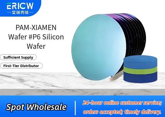
Single-crystal Czochralski (CZ)-grown silicon with ultra-low oxygen and carbon impurity levels.
Double-side polished surface meeting SEMI Standard PV17 for reflectivity and micro-roughness (Ra < 0.2 nm).
High resistivity uniformity (±3% across wafer diameter) suitable for precision device fabrication.
Controlled crystallographic orientation: (100) ±0.5°, optimized for CMOS and MEMS processing.
Free of intentional metallic dopants; background doping enables customizable ion implantation.
Semiconductor prototyping and low-volume IC fabrication in university and R&D cleanrooms.
MEMS sensor substrates requiring high mechanical stability and thermal conductivity.
Photovoltaic research platforms, including heterojunction (HJT) and TOPCon cell development.
Power device test vehicles for Si-based IGBTs and MOSFETs under high-voltage stress conditions.
Calibration reference wafers for ellipsometry, XRR, and AFM metrology systems.
| Chemical Type | Ultra-pure monocrystalline silicon (Si), electronic grade (99.9999999% / 9N) |
| Product Form | Round wafer, prime-grade, double-side polished |
| Appearance | Transparent grayish metallic disc with mirror-like surfaces and beveled edge |
| Diameter | 150 mm (6 inches) ±0.2 mm |
| Thickness | 675 µm ±25 µm |
| Crystallographic Orientation | (100) ±0.5° |
| Resistivity Range | 1–100 Ω·cm (as specified per order; default: 10–20 Ω·cm) |
| Surface Finish | Front: SSP (Standard Surface Polish); Back: Lapped or SSP per requirement |
| Common Compatible Systems | Suitability |
| Applied Materials Centura® Platform | Highly Recommended – Fully compatible with oxide deposition, annealing, and etch modules |
| ASM International PECVD Systems (e.g., Eagle XP8) | Highly Recommended – Verified for SiNₓ and SiO₂ film uniformity on #P6 wafers |
| KLA-Tencor Archer™ Overlay Metrology Tools | Recommended – Supports alignment mark detection and overlay accuracy validation |
| Hitachi SU8000 Series SEM | Suitable – Enables high-resolution cross-sectional imaging with standard conductive coating |
Q1: Does PAM-XIAMEN Wafer #P6 have a CAS Registry Number?
A: Elemental silicon (CAS No. 7440-21-3) applies to the base material; however, as a fabricated semiconductor wafer, #P6 does not carry a unique CAS number — it is classified under HS Code 8541.21 and regulated as an electronic substrate.
Q2: What is the recommended handling protocol to prevent surface contamination during processing?
A: Use Class 100 cleanroom protocols: handle only with Grade 1 lint-free gloves, store in SMIF pods, and perform RCA-1/RCA-2 cleaning prior to lithography or thin-film deposition.
Q3: How does #P6 compare to standard test wafers in terms of particle generation and outgassing in vacuum systems?
A: #P6 undergoes extended post-polish bake (200°C/2h in N₂) and meets SEMI F57 particle limits (<10 particles ≥0.12 µm/cm²); outgassing rate is <1×10⁻⁹ Torr·L/s·cm² per ASTM E1559, making it suitable for UHV-compatible tools.
Q4: Are extraction studies available for potential leachables when used in wet chemical processing (e.g., KOH, TMAH)?
A: Yes — certified analytical reports confirm <0.1 ppb total metallic leachables (Fe, Cu, Ni, Cr, Al) after 10-min immersion in 25% TMAH at 80°C, per ICP-MS testing (certified to ISO/IEC 17025).
Contact With Us:
E-mail: wangxingqiang@ericwchem.com
Have a Questions? Call Us:
Add:
Building A1, Jiete Industrial Park, Huangpu District, Guangzhou City, Guangdong Province, China