English
 Español
 tiếng việt
 русский
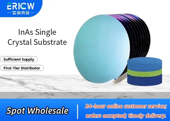
High-purity single-crystal structure with low dislocation density (< 5 × 10⁴ cm⁻²) for superior epitaxial growth fidelity.
Excellent electron mobility (> 30,000 cm²/V·s at 300 K) enabling high-speed and low-noise electronic devices.
Natural (100) crystal orientation with controlled off-cut angles (±0.1°) for optimized heteroepitaxy of III–V compound semiconductors.
Chemically stable surface after standard RCA cleaning, supporting reliable thin-film deposition and device fabrication.
Consistent wafer flatness (TTV < 1.0 µm) and surface roughness (Ra < 0.2 nm), verified by atomic force microscopy (AFM).
Epitaxial growth platform for high-electron-mobility transistors (HEMTs) and quantum cascade lasers (QCLs).
Substrate for infrared photodetectors operating in the 3–5 µm mid-wave infrared (MWIR) spectral range.
Base material for monolithic integration of InAs-based quantum dots and nanowires in quantum computing research.
Template for molecular beam epitaxy (MBE) and metalorganic chemical vapor deposition (MOCVD) of InGaAs/InAlAs heterostructures.
Reference substrate in semiconductor metrology and calibration of X-ray diffraction (XRD) and photoluminescence (PL) systems.
| Chemical Type | Indium Arsenide (InAs), ultra-high purity (99.9999% / 6N) |
| Product Form | Polished single-crystal wafer (round, diameter: 2", 3", or 4") |
| Crystal Orientation | (100) ± 0.1°, with optional 2° off-cut toward [110] |
| Surface Finish | Double-side polished; epi-ready front surface (Ra < 0.2 nm), backside etched or ground |
| Melting Point | 942 °C (inert atmosphere) |
| Primary Applications | III–V optoelectronics, IR detectors, high-frequency electronics, quantum materials research |
| Key Features | Direct bandgap (0.35 eV at 300 K), narrow bandgap, high intrinsic carrier concentration |
| Regulatory Compliance | RoHS-compliant; no intentional addition of REACH SVHC substances |
| Common Compatible Systems | Suitability |
| Veeco Gen10 MBE System | Highly Recommended – Optimized for InAs substrate loading, temperature ramping, and As overpressure control |
| Aixtron Crius II MOCVD Reactor | Recommended – Requires customized InAs-specific precursor delivery and purge protocols |
| Keysight B1500A Semiconductor Parameter Analyzer | Suitable – Validated for DC and pulsed IV characterization of InAs-based FETs and diodes |
| BRUKER D8 DISCOVER XRD System | Highly Recommended – Pre-configured InAs lattice parameter and rocking curve analysis modules |
Q1: What is the CAS Registry Number for InAs?
A: The CAS Number for indium arsenide (InAs) is 12055-87-5.
Q2: Is InAs substrate suitable for aqueous processing or wet chemical etching?
A: InAs is susceptible to oxidation and hydrolysis in ambient air and water; all processing must be performed under inert atmosphere or using non-aqueous, anhydrous etchants (e.g., bromine-methanol or HCl-isopropanol).
Q3: How does InAs compare to GaSb and InSb substrates for MWIR detector applications?
A: InAs offers higher electron mobility and better thermal stability than InSb, and a more favorable lattice match to critical absorber layers (e.g., InAsSb) than GaSb—making it preferred for high-operating-temperature (HOT) MWIR focal plane arrays.
Q4: Are there any known extractables or leachables from InAs wafers during device fabrication?
A: Trace indium and arsenic species may be detected under aggressive acidic cleaning (e.g., concentrated HCl); however, standard RCA-1/RCA-2 followed by dilute HF dip yields extractable levels below 1 ppb per ICP-MS testing—well within semiconductor process control limits.
Q5: Does your InAs substrate carry ISO 9001 or IATF 16949 certification?
A: Our InAs substrate manufacturing process is certified to ISO 9001:2015; IATF 16949 applies only to automotive component production and is not applicable to bare semiconductor substrates.
Contact With Us:
E-mail: wangxingqiang@ericwchem.com
Have a Questions? Call Us:
Add:
Building A1, Jiete Industrial Park, Huangpu District, Guangzhou City, Guangdong Province, China