English
 Español
 tiếng việt
 русский
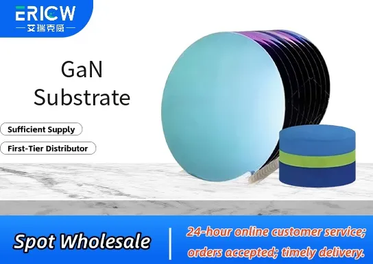
High thermal conductivity (≈ 130–230 W/m·K) enabling efficient heat dissipation in high-power devices.
Wide bandgap (3.4 eV) supporting operation at high voltages, frequencies, and temperatures.
Chemical inertness and excellent resistance to acid/alkali corrosion under standard processing conditions.
Low dislocation density (< 1 × 10⁶ cm⁻²) on homoepitaxial growth surfaces for high device yield.
Single-crystal wurtzite structure with precise lattice matching to GaN-based epitaxial layers.
High-electron-mobility transistors (HEMTs) for 5G RF power amplifiers and base station infrastructure.
Laser diodes and UV LEDs operating in the 365–405 nm range for industrial curing and disinfection.
Power electronics modules in electric vehicles (EVs), onboard chargers, and DC–DC converters.
Satellite communication systems requiring radiation-hardened, high-efficiency semiconductor platforms.
Advanced optoelectronic sensors for aerospace and defense applications under extreme thermal cycling.
| Chemical Type | Gallium Nitride (GaN), ultra-high-purity single crystal |
| Product Form | Polished wafer (double-side polished, EPI-ready surface) |
| Appearance | Transparent to pale yellow, mirror-finish, no visible pits or scratches |
| Melting Point | Decomposes > 2500 °C (no true melting point under atmospheric pressure) |
| Primary Applications | Homoepitaxial growth of GaN-based electronic & optoelectronic devices |
| Key Features | Low threading dislocation density, high crystalline quality, controlled off-axis orientation (0.5°–2°) |
| Benefits | Enables higher breakdown voltage, lower on-resistance, and improved device reliability vs. heteroepitaxial substrates |
| Regulatory Compliance | RoHS 2015/863/EU compliant; REACH SVHC-free; no intentional use of conflict minerals |
| Common Compatible Systems | Suitability |
| MOCVD (Metalorganic Chemical Vapor Deposition) | Highly Recommended – Optimized for GaN-on-GaN epitaxy with minimal interfacial defects |
| Molecular Beam Epitaxy (MBE) | Highly Recommended – Enables precise stoichiometric control and low-temperature growth |
| Ion Implantation & Annealing Systems | Recommended – Compatible with standard activation protocols for dopant incorporation |
| Wafer Bonding Platforms (e.g., plasma-assisted direct bonding) | Suitable – Requires surface activation but achieves strong interfacial adhesion |
Q1: Does GaN substrate have a CAS Registry Number?
A: Yes — Gallium Nitride is assigned CAS No. 25617-97-4. This applies to the bulk crystalline material used as substrate wafers.
Q2: Is GaN substrate subject to migration or leaching in aqueous or humid environments?
A: No — GaN is thermodynamically stable and exhibits negligible dissolution or ion release in neutral water or ambient humidity; hydrolysis requires strongly acidic/alkaline conditions above 100 °C.
Q3: How does GaN substrate compare to sapphire or SiC substrates for high-frequency power devices?
A: GaN substrates eliminate lattice mismatch and thermal expansion coefficient differences present in heteroepitaxial systems, resulting in superior electron mobility, lower dynamic on-resistance, and enhanced thermal management versus sapphire or SiC.
Q4: Are GaN substrates certified for use in medical or food-contact electronic components?
A: While GaN itself is chemically stable and non-toxic, substrate wafers are not classified as finished medical or food-contact materials. Device-level biocompatibility and regulatory approval must be validated separately per IEC 60601 or FDA 21 CFR Part 170–189 requirements.
Contact With Us:
E-mail: wangxingqiang@ericwchem.com
Have a Questions? Call Us:
Add:
Building A1, Jiete Industrial Park, Huangpu District, Guangzhou City, Guangdong Province, China