English
 Español
 tiếng việt
 русский
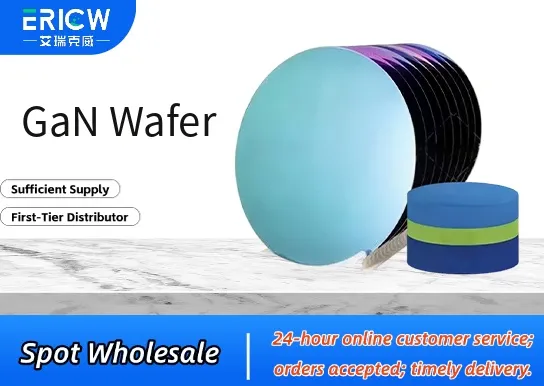
High thermal conductivity (≈ 130–230 W/m·K) enabling efficient heat dissipation in high-power devices.
Wide bandgap (3.4 eV) supporting high-voltage operation and reduced leakage current.
Exceptional chemical stability — resistant to acids, alkalis, and high-temperature oxidation up to 1000 °C in inert atmospheres.
Low intrinsic defect density with dislocation densities < 1 × 10⁸ cm⁻² on optimized templates.
Available on scalable substrates including sapphire (Al₂O₃), silicon carbide (SiC), and silicon (Si) with controlled strain management.
High-electron-mobility transistors (HEMTs) for 5G RF power amplifiers and base station infrastructure.
Power conversion systems including EV onboard chargers, fast DC-DC converters, and industrial SMPS.
UV-A/UV-C optoelectronic emitters and photodetectors for sensing and disinfection applications.
Laser diodes for next-generation displays, automotive LiDAR, and optical communications.
High-frequency millimeter-wave (mmWave) integrated circuits operating beyond 30 GHz.
| Chemical Type | Gallium Nitride (GaN), epitaxial layer on heterogeneous substrate |
| Product Form | Polished, double-side polished (DSP) or single-side polished (SSP) wafer |
| Standard Diameter | 2-inch, 4-inch, and 6-inch (custom sizes available) |
| Typical Thickness | GaN epilayer: 1–6 µm; Total wafer thickness: 350–675 µm (substrate-dependent) |
| Crystal Orientation | (0001) c-plane, semi-polar (e.g., (11-22)), or non-polar (e.g., (11-20)) options |
| Surface Finish | RMS roughness < 0.2 nm (as-measured by AFM over 5 × 5 µm²) |
| Key Features | Controlled doping (Si for n-type, Mg for p-type), low carbon/oxygen contamination (< 1 × 10¹⁷ cm⁻³) |
| Regulatory Compliance | RoHS 2015/863 compliant; REACH SVHC-free; no intentional use of PFAS or conflict minerals |
| Common Compatible Systems | Suitability |
| MOCVD Reactors (e.g., AIXTRON G3, Veeco K465i) | Highly Recommended – Optimized for GaN growth kinetics and uniformity control |
| MBE Systems (e.g., Riber Compact 21, SVT Associates MBE-450) | Recommended – Requires ultra-high vacuum and precise flux calibration |
| Plasma-Enhanced CVD (PECVD) for passivation layers | Suitable – Compatible with SiNₓ and Al₂O₃ deposition for surface passivation |
| ICP-RIE Etch Tools (e.g., Oxford PlasmaLab 100) | Highly Recommended – Enables anisotropic etching with Cl₂/BCl₃ chemistries |
Q1: What is the CAS Registry Number for gallium nitride?
A: Gallium nitride (GaN) has CAS No. 25617-97-4. Note: This number applies to bulk GaN powder; epitaxial wafers are device-grade products and not assigned separate CAS numbers.
Q2: Is GaN wafer subject to migration or leaching under operational conditions?
A: No measurable migration occurs under standard semiconductor processing or device operation. GaN is chemically inert and does not dissolve or leach in ambient air, moisture, or typical packaging environments. Long-term reliability testing shows no detectable Ga or N ion release below 85 °C/85% RH per JEDEC JESD22-A108.
Q3: How does GaN compare to silicon carbide (SiC) for high-power switching applications?
A: GaN offers higher electron mobility and faster switching speeds (sub-nanosecond transitions), making it ideal for frequencies > 1 MHz and compact topologies. SiC excels in higher blocking voltages (> 1.7 kV) and extreme temperature tolerance (> 200 °C junction). Selection depends on system-level trade-offs between frequency, voltage, thermal design, and cost.
Q4: Are your GaN wafers certified for aerospace or automotive qualification standards?
A: Our wafers meet foundational material specifications referenced in AEC-Q200 and ESA/SCC Basic Specification No. 22900. Full component-level qualification (e.g., AEC-Q101) is performed by downstream device manufacturers; we provide full traceability, lot-level test reports, and process documentation to support customer qualification efforts.
Contact With Us:
E-mail: wangxingqiang@ericwchem.com
Have a Questions? Call Us:
Add:
Building A1, Jiete Industrial Park, Huangpu District, Guangzhou City, Guangdong Province, China