English
 Español
 tiếng việt
 русский
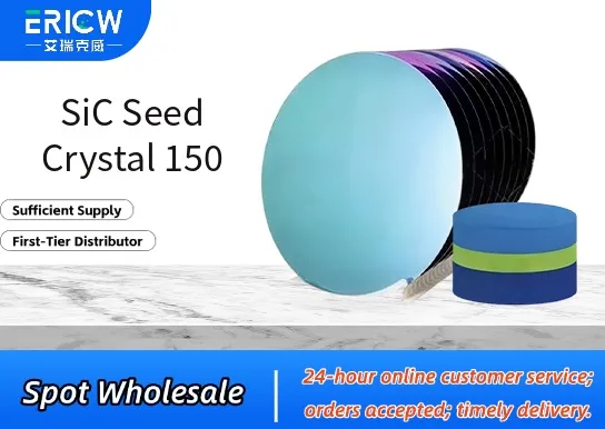
High-purity single-crystal silicon carbide substrate with low dislocation density (< 100 cm⁻²) for reliable homoepitaxial growth.
Optimized 150 mm (6-inch) diameter geometry enabling scalable production of high-quality SiC wafers.
Polished, on-axis (0001) C-face or Si-face orientation available per customer specification.
Controlled surface roughness (< 0.2 nm RMS) and stringent particle contamination control (≤ 5 particles/mm² @ ≥0.3 µm).
Traceable lot documentation including XRD rocking curve data, EPD maps, and surface inspection reports.
Growth of high-voltage, high-frequency SiC power devices (MOSFETs, Schottky diodes, JFETs).
Research and development of wide-bandgap semiconductor heterostructures and quantum materials.
Manufacturing of SiC-based RF components for 5G infrastructure and aerospace radar systems.
Epitaxial template for GaN-on-SiC hybrid platforms requiring thermal stability and lattice matching.
Calibration and reference standard in high-temperature crystal growth process validation.
| Chemical Type | Silicon Carbide (SiC), 4H polytype (standard), 6H optionally available |
| Product Form | Free-standing single-crystal wafer |
| Dimensions | 150 mm (6 inch) nominal diameter, ±0.2 mm; thickness: 350 ± 25 µm |
| Crystal Orientation | (0001) Si-face or (000-1) C-face, off-angle options: 0°, 4°, or 8° toward <11-20> |
| Surface Finish | Double-side polished (DSP), epi-ready front surface |
| Primary Applications | Homoepitaxial SiC wafer manufacturing, R&D seed substrates |
| Key Features | Low micropipe density (< 0.1 cm⁻²), uniform resistivity (≥10⁴ Ω·cm), minimal basal plane dislocation propagation |
| Regulatory Compliance | RoHS 2015/863/EU compliant; REACH SVHC-free; no conflict minerals used |
| Common Compatible Systems | Suitability |
| ABB Crystal Growth Furnace (CGF) Series | Highly Recommended – Optimized thermal profile and gas flow compatibility for PVT growth |
| II-VI (now Coherent) Aixtron G3™ PVT Reactor | Highly Recommended – Verified alignment with 150 mm carrier design and temperature uniformity requirements |
| Topgan TG-150 Epitaxy Platform | Recommended – Supports full 150 mm wafer handling with integrated in-situ monitoring |
| KORRIGAN SiC-GrowPro™ System | Suitable – Requires minor chamber insert adaptation; validated for seeding up to 150 mm |
Q1: What is the CAS Registry Number for SiC Seed Crystal 150?
A: Silicon carbide as a crystalline material does not have a unique CAS number assigned to seed-grade wafers; the base compound SiC is listed under CAS 409-21-2. Product-specific traceability is provided via internal lot ID and QC certificate.
Q2: What is the recommended usage life or reuse limit per SiC Seed Crystal 150 wafer?
A: SiC seed crystals are designed for single-use in primary PVT growth cycles. Reuse is not recommended due to potential surface degradation, carbon segregation, and defect accumulation after high-temperature exposure (>2200 °C).
Q3: How does SiC Seed Crystal 150 differ from standard SiC substrates used for device fabrication?
A: Unlike device-grade substrates, SiC Seed Crystal 150 features enhanced crystal perfection (lower EPD), tighter thickness uniformity, and specialized surface preparation optimized for epitaxial layer nucleation—not electrical performance or backside metallization.
Q4: Are there any known extractables or leachables from SiC Seed Crystal 150 during high-temperature growth?
A: No significant elemental migration occurs under standard PVT conditions. SiC is chemically inert above 1600 °C in argon/vacuum environments; ICP-MS analysis of post-growth chamber residues shows <0.1 ppb Si or C release attributable to the seed itself.
Contact With Us:
E-mail: wangxingqiang@ericwchem.com
Have a Questions? Call Us:
Add:
Building A1, Jiete Industrial Park, Huangpu District, Guangzhou City, Guangdong Province, China