English
 Español
 tiếng việt
 русский
Single-crystal structure with high optical homogeneity and low scattering loss.
Exceptional electro-optic coefficient (r₃₃ ≈ 30 pm/V), enabling efficient high-speed modulation.
Wide optical transparency range from 350 nm to 5.5 μm, supporting UV–mid-IR applications.
High Curie temperature (~1140 °C), ensuring thermal stability during device fabrication and operation.
Chemically inert and mechanically robust, compatible with standard cleanroom processing (e.g., photolithography, etching, thin-film deposition).
Integrated photonic circuits for telecom and datacom transceivers (e.g., Mach–Zehnder modulators).
Surface acoustic wave (SAW) and bulk acoustic wave (BAW) filters in RF front-end modules.
Nonlinear optical devices including second-harmonic generation (SHG), optical parametric oscillators (OPOs), and difference-frequency generation (DFG).
Electro-optic sensors for electric field sensing, voltage monitoring, and ultrafast diagnostics.
Quantum photonics platforms, including entangled photon sources and reconfigurable interferometers.
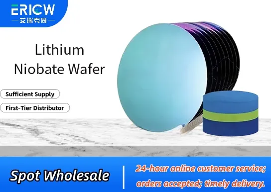
| Chemical Type | Lithium niobate (LiNbO₃), congruent or stoichiometric composition |
| Product Form | Polished double-side wafers (standard thickness: 0.5 mm, 1.0 mm) |
| Crystal Orientation | Z-cut, X-cut, Y-cut, or custom orientation (±0.5° tolerance) |
| Surface Finish | Double-side polished; RMS roughness < 0.3 nm; epi-ready quality |
| Primary Applications | Photonic integrated circuits, RF filters, nonlinear optics, quantum devices |
| Key Features | High electro-optic & piezoelectric coefficients; excellent birefringence control; low propagation loss (< 0.1 dB/cm @ 1550 nm) |
| Benefits | Enables monolithic integration of active/passive functions; supports heterogeneous bonding (e.g., LNOI – Lithium Niobate on Insulator) |
| Regulatory Compliance | RoHS 2015/863 compliant; REACH SVHC-free; no conflict minerals used in substrate manufacturing |
| Common Compatible Systems | Suitability |
| Lithium Niobate on Insulator (LNOI) platform | Highly Recommended – Designed for direct bonding and etch-transfer processes |
| Standard silicon photonics foundry processes (e.g., AMF, IMEC, AIM Photonics) | Recommended – Compatible with hybrid integration via flip-chip or micro-transfer printing |
| RF sputtering & e-beam evaporation systems (e.g., Kurt J. Lesker, Angstrom Engineering) | Highly Recommended – Stable under vacuum deposition of metal electrodes (Au, Ti/Au, Cr/Au) |
| Reactive ion etching (RIE) tools with CHF₃/Ar or Cl₂-based chemistries | Suitable – Requires optimized power/duration to minimize surface damage and redeposition |
Q1: What is the CAS Registry Number for lithium niobate?
A: The CAS number for lithium niobate (LiNbO₃) is 12031-64-4.
Q2: Is lithium niobate wafer subject to leaching or ion migration under operational conditions?
A: No significant leaching occurs under ambient or typical optoelectronic operating conditions (≤85 °C, non-aqueous environments); however, prolonged exposure to humid or acidic environments may induce surface hydrolysis — protective passivation (e.g., SiO₂ capping) is recommended for harsh environments.
Q3: How does congruent lithium niobate compare to stoichiometric lithium niobate in performance?
A: Stoichiometric LiNbO₃ exhibits ~2× higher electro-optic coefficients, lower coercive field, reduced photorefractive damage, and improved domain engineering fidelity compared to congruent material — ideal for high-power and domain-inverted devices.
Q4: Are lithium niobate wafers certified for use in medical or aerospace-grade applications?
A: Wafers are supplied with full traceability and material test reports (MTRs); qualification for specific medical (ISO 13485) or aerospace (AS9100) applications requires customer-driven device-level validation — we support with lot-specific certificates of conformance and controlled packaging.
Contact With Us:
E-mail: wangxingqiang@ericwchem.com
Have a Questions? Call Us:
Add:
Building A1, Jiete Industrial Park, Huangpu District, Guangzhou City, Guangdong Province, China