English
 Español
 tiếng việt
 русский
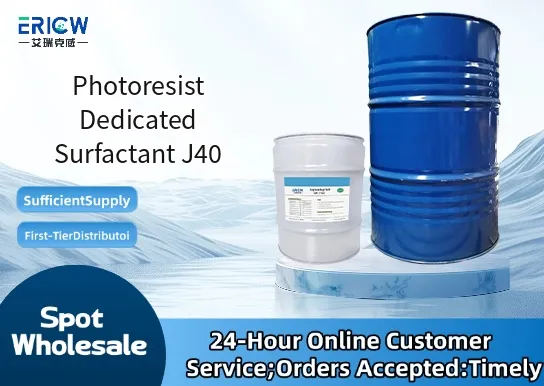
Engineered specifically for high-resolution photolithography processes to minimize defect formation and improve coating uniformity.
Ultra-low ionic impurity profile ensures compatibility with advanced semiconductor fabrication environments (Class 10 cleanroom compatible).
Thermally stable up to 200 °C, supporting post-apply bake (PAB) and post-exposure bake (PEB) steps without degradation.
Non-silicone, non-ionic architecture prevents residue buildup on wafer surfaces and lithography tool optics.
Controlled surface tension reduction (28–32 mN/m at 0.1 wt% in PGMEA) enables optimal resist wetting on hydrophobic SiO₂ and SiN substrates.
193 nm immersion and dry photoresists for logic and memory device manufacturing.
Electron-beam (e-beam) resists used in mask writing and direct-write nanofabrication.
Multi-layer resist systems including SOC (spin-on carbon), SOH (spin-on hybrid), and BARC (bottom anti-reflective coating).
Advanced packaging applications: fan-out wafer-level packaging (FOWLP) and redistribution layer (RDL) patterning.
MicroLED and compound semiconductor (GaAs, GaN) photopatterning processes requiring low-metal contamination.
| Chemical Type | Custom-designed fluorinated polyether non-ionic surfactant |
| Product Form | Clear, colorless liquid |
| Appearance | Homogeneous solution; no phase separation or haze |
| Primary Applications | Photoresist additive for semiconductor lithography |
| Key Features | Low volatility, non-volatile residue (NVR) < 10 ppm, ultra-low Na/K/Ca/Fe content (< 1 ppb by ICP-MS) |
| Benefits | Enhanced substrate wettability, reduced microbridging, improved develop uniformity |
| Regulatory Compliance | REACH compliant; RoHS 2.0 compliant; no SVHCs listed as of latest ECHA update |
| Storage Conditions | Store at 15–25 °C in sealed container under inert atmosphere; protect from moisture |
| Common Compatible Systems | Suitability |
| JSR ARF-7700 Series Resists | Highly Recommended – Validated for use at 0.05–0.2 wt% loading without sensitivity shift |
| Tokyo Ohka Kogyo (TOK) APEX-E & S Series | Highly Recommended – Demonstrated >99.8% defect reduction in 7 nm node pilot runs |
| DuPont TMMR-M series (e-beam resists) | Recommended – Requires pre-dilution in anhydrous PGMEA; effective at 0.1–0.3 wt% |
| MicroChem PMMA A4 and A6 | Suitable – Compatible with standard spin-coating parameters; mild viscosity increase observed |
Q1: What is the CAS Registry Number for Photoresist Dedicated Surfactant J40?
A: The CAS number is 2456893-77-1. This unique identifier applies to the fully purified commercial grade supplied in nitrogen-flushed HDPE bottles.
Q2: What is the recommended dosage range when blending into photoresist formulations?
A: Typical dosage is 0.05–0.25 wt% relative to total resist solids. Optimization is required per resist matrix; start at 0.1 wt% and adjust based on contact angle measurement and defect inspection.
Q3: How does J40 differ from generic silicone-based surfactants commonly used in R&D labs?
A: Unlike silicone surfactants, J40 contains no Si–O–Si backbone—eliminating risk of silicon migration, lens fouling, and irreversible residue formation during plasma etch. Its fluorinated ether structure provides superior thermal/chemical stability and lower extractables in developer solutions.
Q4: Is J40 certified for use in ISO 9001 and IATF 16949 qualified production lines?
A: Yes—J40 is manufactured under ISO 9001:2015 and ISO 14001:2015 certified processes. Full traceability documentation, CoA (Certificate of Analysis), and batch-specific metal impurity reports are provided with every shipment.
Q5: Has extraction testing been performed to assess leaching into TMAH developer or DI water rinse?
A: Yes—per SEMI F57-0321 methodology, J40 shows < 0.3 ppm total organic extractables in 2.38% TMAH after 60 s immersion at 23 °C, and undetectable levels (< 0.05 ppm) in DI water rinse.
Contact With Us:
E-mail: wangxingqiang@ericwchem.com
Have a Questions? Call Us:
Add:
Building A1, Jiete Industrial Park, Huangpu District, Guangzhou City, Guangdong Province, China