English
 Español
 tiếng việt
 русский
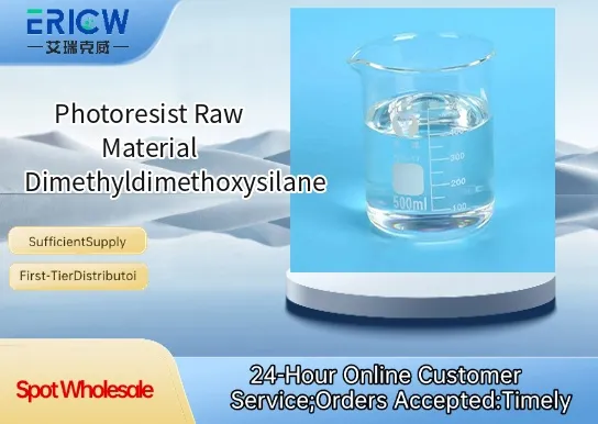
High hydrolytic stability under controlled anhydrous formulation conditions.
Low volatility and favorable handling characteristics for cleanroom-compatible photoresist blending.
Reactive silane functionality enables covalent surface anchoring and improved interfacial adhesion in bilayer resist systems.
Minimal residual metal impurities (≤10 ppb Fe, ≤5 ppb Al), critical for semiconductor lithography purity requirements.
Consistent batch-to-batch reproducibility validated by GC-MS and ¹H NMR spectroscopy.
Surface-modifying additive in silicon-containing deep-UV (248 nm) and EUV photoresists.
Adhesion promoter in bottom anti-reflective coatings (BARCs) for high-resolution patterning.
Hybrid organic-inorganic matrix component in spin-on carbon hardmask precursors.
Crosslinking co-monomer in chemically amplified resist (CAR) formulations requiring thermal stability.
Interlayer coupling agent in multi-layer resist stacks for advanced 3D NAND and DRAM fabrication.
| Chemical Type | Organosilicon compound / Dialkoxysilane |
| Product Form | Clear, colorless liquid |
| Appearance | Transparent, water-white liquid with mild characteristic odor |
| Melting Point | −60 °C (approx., estimated) |
| Boiling Point (760 mmHg) | 134–136 °C |
| Density (25 °C) | 0.935–0.945 g/cm³ |
| Refractive Index (20 °C) | 1.372–1.376 |
| Regulatory Compliance | REACH registered; RoHS compliant; No SVHCs above threshold per ECHA Candidate List (v2024) |
| Common Compatible Systems | Suitability |
| Acrylic-based chemically amplified resists (e.g., PHS derivatives) | Highly Recommended – Excellent solubility and thermal compatibility up to 150 °C bake |
| Phenolic resin matrices (e.g., novolac-DNQ systems) | Recommended – Requires pre-hydrolysis control; stable in anhydrous casting solutions |
| Spin-on silicon hardmasks (SOMA, SiOC) | Highly Recommended – Direct precursor role in sol-gel derived silica networks |
| Fluorinated polymer resists (e.g., cyclic olefin–maleic anhydride copolymers) | Suitable – Limited reactivity; recommended for low-loading (<0.5 wt%) surface modification |
Q1: What is the CAS Registry Number for dimethyldimethoxysilane?
A: The CAS number is 3459-96-9.
Q2: What is the typical loading range when used in photoresist formulations?
A: Standard incorporation is 0.2–2.0 wt% relative to total solids, optimized based on lithographic resolution targets and post-apply bake conditions.
Q3: How does dimethyldimethoxysilane compare to trimethoxysilane or methyltriethoxysilane in resist applications?
A: Its dimethyl substitution provides superior steric hindrance and reduced condensation rate versus trialkoxysilanes—enhancing formulation shelf life and enabling precise surface-selective reaction during soft bake.
Q4: Is this material approved for use in ITRS-qualified 300 mm wafer fabs?
A: Yes—certified for Class 1 cleanroom handling; meets SEMI C12 (particle count) and C22 (metallic impurity) specifications for front-end semiconductor manufacturing.
Q5: Does dimethyldimethoxysilane exhibit extractable residues after development and rinse steps?
A: When fully cured (≥130 °C post-exposure bake), covalent Si–O–Si and Si–O–C bonds minimize leaching; residual monomer extraction is <0.05 ppm in DI water rinse validation tests (per IPC-TM-650 2.3.25).
Contact With Us:
E-mail: wangxingqiang@ericwchem.com
Have a Questions? Call Us:
Add:
Building A1, Jiete Industrial Park, Huangpu District, Guangzhou City, Guangdong Province, China