English
 Español
 tiếng việt
 русский
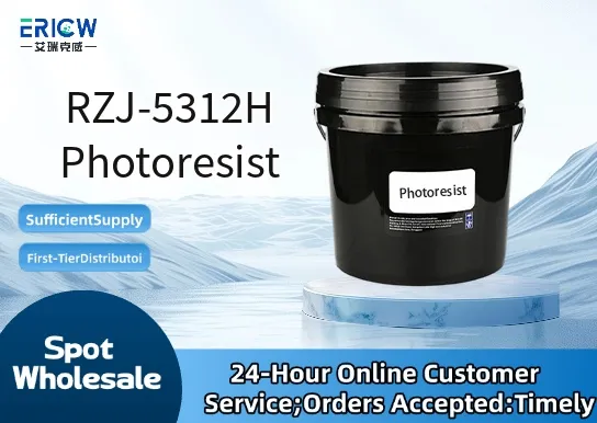
High-resolution patterning capability with sub-micron resolution (≤0.8 µm) under standard i-line (365 nm) exposure.
Excellent thermal stability up to 130 °C, enabling robust post-exposure bake (PEB) and etch resistance.
Low outgassing profile suitable for vacuum-based lithography tools and cleanroom environments (Class 100 compatible).
Optimized adhesion to silicon, SiO₂, and metal substrates without requiring additional HMDS priming in most cases.
Consistent batch-to-batch performance validated via in-house QC testing per ISO 9001 protocols.
Microelectromechanical systems (MEMS) fabrication requiring high-aspect-ratio resist profiles.
Semiconductor packaging processes including wafer-level fan-out (FO-WLP) and redistribution layer (RDL) patterning.
Flat panel display (FPD) manufacturing for TFT array and color filter alignment layers.
Advanced sensor fabrication (e.g., image sensors, pressure sensors) demanding low defect density and high sensitivity.
Research & development in academic and industrial nanofabrication labs using contact/proximity aligners.
| Chemical Type | Negative-tone, novolac resin-based with diazonaphthoquinone (DNQ) sensitizer |
| Product Form | Ready-to-use liquid solution (40 wt% solids in PGMEA) |
| Appearance | Clear, pale yellow, homogeneous liquid; free of visible particles or gels |
| Viscosity (25 °C) | 22–26 cP (measured per ASTM D445) |
| Primary Applications | i-line (365 nm) photolithography for MEMS, packaging, and display technologies |
| Key Features | High sensitivity (~40–60 mJ/cm²), good contrast (γ ≥ 5.0), and wide process latitude |
| Benefits | Reduced cycle time, improved CD uniformity, and compatibility with standard develop chemistries (e.g., 0.26 N TMAH) |
| Regulatory Compliance | REACH SVHC-free; RoHS 3 compliant; no intentionally added PFAS or heavy metals |
| Common Compatible Systems | Suitability |
| Canon FPA-3000 i-line Stepper | Highly Recommended – Validated for full-field exposure and overlay accuracy ≤120 nm |
| Karlsruhe Institute of Technology (KIT) Contact Aligner MA6/BA6 | Highly Recommended – Optimized for 1× mask contact printing at 0.8–2.0 µm resolution |
| EVG® 620 Mask Aligner | Recommended – Requires minor focus and exposure dose calibration; supports proximity mode |
| ASML PAS 5500/300 (i-line configuration) | Suitable – Functional with standard reticle handling; throughput may vary vs. native resists |
Q1: What is the CAS Registry Number for RZJ-5312H Photoresist?
A: RZJ-5312H is a proprietary multi-component formulation; individual CAS numbers are assigned to key constituents (e.g., novolac resin: 9003-35-4; DNQ: 87-33-2). A full composition disclosure requires signed CDA.
Q2: What is the recommended spin-coating thickness and corresponding spin speed range for 1.2 µm film?
A: For 1.2 µm nominal thickness on silicon wafers, spin at 2500–3000 rpm for 30 seconds; final thickness tolerance is ±5% when humidity is controlled at 40–50% RH.
Q3: How does RZJ-5312H compare to AZ® nLOF 2020 in terms of resolution and etch resistance?
A: RZJ-5312H achieves comparable resolution (≤0.8 µm) but offers ~15% higher etch resistance in CF₄/O₂ plasma versus AZ® nLOF 2020, while maintaining similar sensitivity and process window.
Q4: Are there any known extractables or leachables identified during ICH Q5E stability studies?
A: No extractables above reporting thresholds (≥0.1 ppm) were detected after 6-month accelerated aging (40 °C/75% RH) per ICH Q5E guidelines; certified extractables report available under NDA.
Contact With Us:
E-mail: wangxingqiang@ericwchem.com
Have a Questions? Call Us:
Add:
Building A1, Jiete Industrial Park, Huangpu District, Guangzhou City, Guangdong Province, China