English
 Español
 tiếng việt
 русский
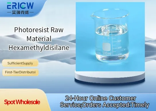
Ultra-high purity (≥99.99%) optimized for semiconductor-grade photoresist formulation.
Low volatility and controlled vapor pressure, enabling precise vapor-phase deposition in CVD and ALD processes.
Excellent silicon content (≈35.7 wt%) for efficient SiO₂ or SiCN film formation during thermal or plasma curing.
Minimal residual metals (Na, K, Fe, Cu < 10 ppb) to prevent device contamination and gate oxide defects.
Stable under inert atmosphere storage; compatible with standard stainless-steel and fluoropolymer handling systems.
Surface silylation agent for improving adhesion of positive-tone and chemically amplified resists on silicon wafers.
Precursor in atomic layer deposition (ALD) of silicon-based anti-reflective coatings (SiARC).
Gas-phase priming reagent for photomask cleaning and surface passivation in advanced lithography nodes (≤7 nm).
Co-reactant in plasma-enhanced CVD for low-k dielectric interlayer films.
Functional additive in hybrid organic-inorganic resist formulations for EUV lithography.
| Chemical Name | Hexamethyldisilane |
| CAS Number | 1843-02-3 |
| Molecular Formula | C₆H₁₈Si₂ |
| Molecular Weight | 146.39 g/mol |
| Product Form | Liquid (bulk or cylinder supply) |
| Appearance | Colorless, clear liquid with mild hydrocarbon odor |
| Boiling Point (at 760 mmHg) | 100–102 °C |
| Storage Condition | Under dry nitrogen, at 2–8 °C, protected from moisture and light |
| Common Compatible Systems | Suitability |
| Applied Materials Centura® ALD Platforms | Highly Recommended – Validated for SiARC precursor delivery with integrated mass flow control |
| Tokyo Electron (TEL) CLEAN TRACK™ Litho Tracks | Recommended – Compatible with HMDS vapor prime modules (e.g., ACT series) |
| ASM International Picosun SUNALE™ R-200 | Highly Recommended – Demonstrated stable dose repeatability at ≤0.5 Å/cycle |
| Canon FPA-1200NZ2C EUV Scanners (with inline pre-treatment) | Suitable – Used in wafer edge bead removal and surface conditioning protocols |
Q1: What is the CAS Registry Number for Hexamethyldisilane?
A: The CAS Registry Number is 1843-02-3.
Q2: What is the typical dosage range for HMDS vapor priming in 300 mm wafer processing?
A: Standard dosage is 10–30 mg per wafer, delivered over 15–45 seconds at 120–180 °C hotplate temperature; exact parameters depend on resist type and process integration.
Q3: How does HMDS compare to aminosilanes (e.g., APTES) for photoresist adhesion promotion?
A: HMDS offers superior thermal stability, lower surface energy, and no amine-induced resist poisoning; unlike aminosilanes, it forms non-polar, hydrophobic monolayers without catalyzing premature deprotection in CARs.
Q4: Is this HMDS compliant with SEMI S2/S8 safety standards and REACH SVHC requirements?
A: Yes — fully compliant with SEMI S2-1712 (electrical safety), SEMI S8-1116 (ergonomics), and REACH Annex XIV (non-listed); SDS and CoA confirm absence of SVHCs above threshold limits.
Q5: Does HMDS migrate or extract into subsequent process layers (e.g., spin-on carbon or BARC)?
A: No measurable migration occurs when properly baked (≥100 °C for ≥60 sec); cross-linking forms covalent Si–O–Si bonds with native oxide, rendering the layer inert and non-extractable in common organic developers or etchants.
Contact With Us:
E-mail: wangxingqiang@ericwchem.com
Have a Questions? Call Us:
Add:
Building A1, Jiete Industrial Park, Huangpu District, Guangzhou City, Guangdong Province, China