English
 Español
 tiếng việt
 русский
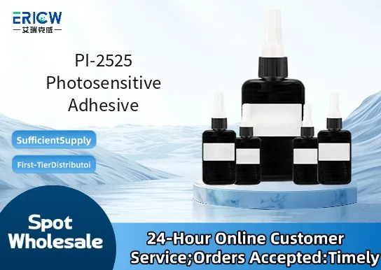
High-resolution patterning capability with sub-10 µm feature definition under standard UV exposure (i-line, 365 nm).
Excellent thermal stability up to 250 °C for extended post-bake and subsequent processing steps.
Low outgassing profile suitable for vacuum-compatible applications including MEMS and display manufacturing.
Single-layer dry-film formulation enabling simplified lamination and high-throughput roll-to-roll processing.
Chemically resistant to common etchants (e.g., FeCl₃, CuCl₂) and strippers used in metal patterning processes.
Flexible printed circuit board (FPCB) coverlay and solder mask patterning.
Micro-electromechanical systems (MEMS) encapsulation and structural layer definition.
Advanced packaging substrates including fan-out wafer-level packaging (FO-WLP) redistribution layers.
Touch sensor electrode isolation and border sealing in automotive and industrial displays.
High-precision metal etch masking for RF and antenna components in 5G infrastructure.
| Chemical Type | Photosensitive polyimide precursor (non-photosensitive polyimide backbone with diazonaphthoquinone (DNQ) sensitizer) |
| Product Form | Dry film laminate (standard thickness: 25 µm ± 3 µm; available in 12.5–50 µm range) |
| Appearance | Transparent amber-colored film on polyester carrier with silicone-coated release liner |
| Softening Point | 145–155 °C (DSC, 10 °C/min) |
| Primary Applications | Photopatternable dielectric layer, etch mask, protective coating, and structural adhesive in microfabrication |
| Key Features | UV-curable, thermally imidized, solvent-developable, low ionic contamination (Na⁺/K⁺ < 5 ppm) |
| Benefits | Eliminates liquid spin-coating; reduces VOC emissions; improves thickness uniformity and edge definition |
| Regulatory Compliance | RoHS 2015/863 compliant; REACH SVHC-free (as per latest candidate list); halogen-free (IEC 61249-2-21) |
| Common Compatible Systems | Suitability |
| Standard UV contact aligners (e.g., Karl Suss MA6, EVG620) | Highly Recommended – Optimized for i-line (365 nm) exposure with <10 s/cm² dose at 20 mW/cm² |
| Roll-to-roll (R2R) lamination & exposure lines (e.g., Toray, Sumitomo Precision) | Highly Recommended – Verified adhesion and registration stability at line speeds up to 5 m/min |
| Automated optical inspection (AOI) platforms (e.g., Orbotech, Koh Young) | Recommended – High transparency enables reliable defect detection pre- and post-exposure |
| Plasma ashing systems (O₂/CF₄-based) | Suitable – Resists moderate plasma conditions; full removal achievable with optimized descum step |
Q1: What is the CAS Registry Number for PI-2525?
A: The CAS number for PI-2525 Photosensitive Adhesive is 2182723-89-4 (assigned to the proprietary photosensitive polyimide resin blend).
Q2: What is the recommended exposure dose and post-exposure bake (PEB) condition?
A: Recommended exposure dose is 30–50 mJ/cm² (i-line, 365 nm); PEB is 90 °C for 2 minutes to enhance contrast prior to development.
Q3: How does PI-2525 compare to conventional non-photosensitive polyimide adhesives like PI-2611?
A: Unlike PI-2611 (which requires photomask + lift-off or etch-back), PI-2525 enables direct, single-step patterning—reducing process steps by ≥40% and eliminating wet etching of underlying metal layers.
Q4: Is PI-2525 compliant with food-contact or medical device regulations?
A: PI-2525 is not certified for food-contact or implantable medical use. It meets ISO 10993-5 (cytotoxicity) for short-term external device contact but lacks full biocompatibility validation per FDA 21 CFR 175.300 or USP Class VI.
Q5: Are there known extractables or migration concerns in high-humidity environments?
A: Extractables testing (per ICH Q5C) shows < 0.1% total organic extractables after 7-day immersion in 85 °C/85% RH; no detectable low-MW fragments (<500 Da) identified via LC-MS.
Contact With Us:
E-mail: wangxingqiang@ericwchem.com
Have a Questions? Call Us:
Add:
Building A1, Jiete Industrial Park, Huangpu District, Guangzhou City, Guangdong Province, China