 English
 Español
 tiếng việt
 русский
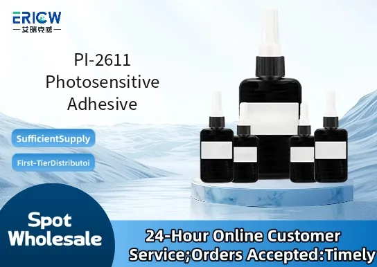
High-resolution photopatternability with sub-15 µm feature definition under standard i-line (365 nm) exposure.
Excellent thermal stability up to 200 °C post-cure, retaining adhesion and dimensional integrity in high-temperature processing.
Low outgassing profile compliant with ISO 15097, suitable for vacuum and cleanroom-sensitive applications.
Chemically resistant to common solvents including acetone, IPA, and dilute alkaline developers (e.g., 0.26 N TMAH).
UV-curable formulation enabling rapid, solvent-free patterning without thermal crosslinking requirements.
Flexible printed circuit (FPC) coverlay lamination and via definition.
Wafer-level packaging (WLP) redistribution layer (RDL) dielectric and bonding adhesive.
Microelectromechanical systems (MEMS) cavity sealing and structural bonding.
Advanced display module bonding for OLED and microLED substrates.
Hermetic encapsulation of high-reliability sensors and RF components.
| Chemical Type | Photosensitive polyimide precursor (acrylate-modified) |
| Product Form | Viscous liquid (spin-coatable, dispensable) |
| Appearance | Amber-transparent, particle-free solution |
| Solvent Content | ~35–40 wt% (NMP-based) |
| Primary Applications | Photopatternable dielectric & structural adhesive |
| Key Features | Positive-tone, self-developing capability after UV exposure |
| Benefits | No separate photoresist required; single-material process integration |
| Regulatory Compliance | RoHS 2015/863 compliant; REACH SVHC Candidate List free (as of 2024) |
| Common Compatible Systems | Suitability |
| i-Line Stepper / Mask Aligner (365 nm) | Highly Recommended – Optimized sensitivity and contrast at 100–300 mJ/cm² |
| Standard Semiconductor Wet Bench (TMAH developer) | Highly Recommended – Full compatibility with 0.26 N aqueous TMAH at 23 °C |
| Hotplate & Vacuum Oven Curing Systems | Recommended – Requires staged cure: 90 °C (pre-bake), 200 °C (post-exposure cure) |
| Plasma Ashing Equipment (O₂/CF₄) | Suitable – Resists mild ashing; extended exposure may cause surface erosion |
Q1: What is the CAS Registry Number for PI-2611?
A: The CAS Number for PI-2611 Photosensitive Adhesive is 2272124-89-1 (for the proprietary polymer blend; individual solvent components are listed separately in the SDS).
Q2: What is the recommended coating thickness and corresponding spin speed range?
A: For 10–25 µm dry film thickness, use 1500–3500 rpm for 30 seconds on silicon or copper substrates; optimal resolution achieved at 15–20 µm with 2500 rpm.
Q3: How does PI-2611 compare to conventional non-photosensitive polyimide adhesives like PI-2610?
A: Unlike PI-2610, PI-2611 eliminates separate photomask and resist steps—enabling direct imaging, reduced process cycle time, and improved registration accuracy for fine-pitch bonding.
Q4: Is PI-2611 compliant with food-contact or medical device regulations?
A: PI-2611 is not certified for food-contact (FDA 21 CFR) or implantable medical devices; it is qualified for industrial electronics per IPC-4101 and JEDEC J-STD-020 standards.
Q5: Are there documented migration or extractables data for PI-2611 under thermal stress?
A: Yes—GC-MS analysis shows <0.05% total volatile condensable material (CVCM) after 24 h at 125 °C per ASTM E595; no detectable low-MW leachables in ICP-MS testing under 85 °C/85% RH for 168 h.
Contact With Us:
E-mail: wangxingqiang@ericwchem.com
Have a Questions? Call Us:
Add:
Building A1, Jiete Industrial Park, Huangpu District, Guangzhou City, Guangdong Province, China

![4-[(2,3-Dihydrothieno[3,4-b]-1,4-Dioxin-2-yl)Methoxy]-1-Butanesulfonic Acid Sodium Salt](/uploads/image/20260922/4-2-3-dihydrothieno-3-4-b-1-4-dioxin-2-yl-methoxy-1-butanesulfonic-acid-sodium-s_fab320bf.webp "4-[(2,3-Dihydrothieno[3,4-b]-1,4-Dioxin-2-yl)Methoxy]-1-Butanesulfonic Acid Sodium Salt")


