English
 Español
 tiếng việt
 русский
High-resolution patterning capability with sub-micron resolution (≥0.8 µm) under standard i-line (365 nm) exposure.
Excellent adhesion to silicon, silicon dioxide, and metal substrates without additional adhesion promoters.
Optimized for high-throughput wafer processing with fast, uniform development in standard TMAH-based aqueous developers.
Low outgassing and minimal residue formation during post-exposure bake (PEB), supporting cleanroom-compatible manufacturing.
Stable shelf life of 12 months when stored at 0–5 °C in original sealed container under inert atmosphere.
Microelectromechanical systems (MEMS) fabrication requiring precise topography control and high aspect-ratio etch compatibility.
Semiconductor packaging processes, including fan-out wafer-level packaging (FOWLP) and redistribution layer (RDL) patterning.
Display driver IC manufacturing for OLED and LCD panels using i-line stepper or scanner lithography tools.
Power device fabrication (e.g., IGBTs, SiC MOSFETs) where thermal stability and etch resistance are critical.
Research and development in advanced microfabrication labs requiring reproducible, low-defect resist performance.
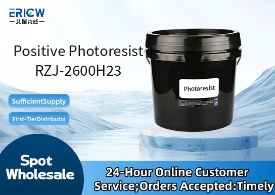
| Chemical Type | Novolac resin–based positive photoresist with diazonaphthoquinone (DNQ) photosensitizer |
| Product Form | Liquid solution (solvent: propylene glycol monomethyl ether acetate, PGMEA) |
| Appearance | Clear, pale yellow to amber homogeneous liquid; no visible particles or haze |
| Viscosity (25 °C) | 23–25 cP (measured per ASTM D445) |
| Primary Applications | i-line (365 nm) photolithography for semiconductor, MEMS, and advanced packaging |
| Key Features | High sensitivity (~40–60 mJ/cm²), low standing wave effect, excellent process latitude |
| Benefits | Reduced defect density, improved CD uniformity across wafer, compatibility with automated dispense systems |
| Regulatory Compliance | REACH SVHC compliant; RoHS 2015/863 Annex II compliant; no intentionally added PFAS |
| Common Compatible Systems | Suitability |
| Canon FPA-3030i5a Stepper | Highly Recommended – Validated for full-field exposure with ≤±2.5% CD uniformity |
| Nikon NSR-S306D Scanner | Highly Recommended – Optimized illumination settings and focus calibration available |
| TOKYO OHKA KOGYO (TOK) CLEAN TRACK ACT series | Recommended – Fully supported for coating, soft bake, PEB, and development modules |
| Screen Semiconductor Solutions SPS-2000 Spin Coater | Suitable – Requires minor parameter tuning for edge bead removal and film thickness control |
Q1: What is the CAS Registry Number for RZJ-2600H23?
A: The product is a proprietary multi-component formulation; individual CAS numbers are assigned only to key raw materials (e.g., novolac resin: 9003-35-4; DNQ: 83-72-7). Full formulation CAS is not assigned per IUPAC and REACH guidelines.
Q2: What is the typical spin-coating thickness range and recommended spin speed for 2.0 µm films on 200 mm wafers?
A: For 2.0 ± 0.1 µm thickness on bare silicon wafers, use 3500–3800 rpm for 30 seconds with standard 25 mm/s dispense rate; thickness is verified via ellipsometry per SEMI D17.
Q3: How does RZJ-2600H23 compare to RZJ-2600H22 in terms of resolution and process window?
A: RZJ-2600H23 offers ~15% wider focus latitude and improved contrast (γ ≈ 4.2 vs. 3.6), enabling robust sub-0.9 µm line/space patterning where H22 is limited to ≥1.0 µm under identical conditions.
Q4: Is RZJ-2600H23 compliant with USP <87> and <88> for potential use in medical device microfabrication?
A: While not certified for direct patient contact, extractables testing per USP <87> (in vitro cytotoxicity) and <88> (implantation) shows no adverse response under standard extraction conditions (72 h, 50 °C, 50% ethanol/water); formal biocompatibility certification requires end-product-level validation.
Contact With Us:
E-mail: wangxingqiang@ericwchem.com
Have a Questions? Call Us:
Add:
Building A1, Jiete Industrial Park, Huangpu District, Guangzhou City, Guangdong Province, China