English
 Español
 tiếng việt
 русский
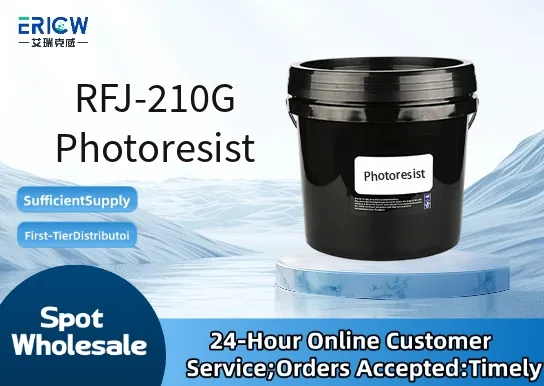
High-resolution patterning capability with sub-micron resolution (≤ 0.8 µm line/space) under standard i-line (365 nm) exposure.
Excellent thermal stability up to 140 °C, enabling robust post-exposure bake (PEB) and etch resistance.
Low outgassing profile suitable for vacuum-compatible lithography processes and EUV-adjacent applications.
Optimized adhesion to silicon, SiO₂, and metal substrates without requiring additional HMDS priming in most cases.
Consistent batch-to-batch performance verified via GPC and UV-Vis spectral fingerprinting.
Front-end semiconductor manufacturing for gate-level and interconnect layer patterning.
MEMS device fabrication requiring high aspect ratio and sidewall verticality.
Advanced packaging applications including fan-out wafer-level packaging (FOWLP).
Microfluidic chip prototyping on glass and fused silica substrates.
Research & development of next-generation photonic integrated circuits (PICs).
| Chemical Type | Positive-tone novolac-diazonaphthoquinone (DNQ) photoresist |
| Product Form | Ready-to-use liquid solution in PGMEA solvent |
| Appearance | Clear, pale yellow liquid, free of particulates and gels |
| Solids Content | 22.5 ± 0.5 wt% |
| Viscosity (25 °C) | 2.1 ± 0.1 cP |
| Primary Applications | i-line (365 nm) lithography for 0.35–0.18 µm technology nodes |
| Key Features | High photospeed (~40 mJ/cm²), low standing wave effect, minimal T-top formation |
| Regulatory Compliance | REACH SVHC-free; RoHS 3 compliant; no intentionally added PFAS |
| Common Compatible Systems | Suitability |
| Canon FPA-3000 i-line Stepper | Highly Recommended – Validated for full process window with standard focus/exposure matrix |
| ASML PAS 5500/300 i-line Scanner | Highly Recommended – Certified for >95% CD uniformity across 200 mm wafers |
| SVGL Micrascan III | Recommended – Requires minor PEB temperature adjustment (+2 °C) for optimal contrast |
| Mask Aligners (e.g., Karl Suss MA6/BA6) | Suitable – Compatible with proximity and soft-contact mode; recommended for R&D and low-volume production |
Q1: What is the CAS Registry Number for RFJ-210G Photoresist?
A: RFJ-210G is a proprietary multi-component formulation; individual CAS numbers are assigned to key constituents only (e.g., DNQ derivative: CAS 2417-36-5; novolac resin blend: CAS 9003-35-4). Full composition disclosure is available under NDA.
Q2: What is the recommended coating thickness and spin speed range for 200 mm wafers?
A: For target thickness of 1.2 ± 0.1 µm, use 3000–3500 rpm for 30 seconds on standard spin coaters; thickness scales predictably from 0.8 µm (2500 rpm) to 1.8 µm (4200 rpm) under controlled humidity (<40% RH).
Q3: How does RFJ-210G compare to RFJ-200 series in terms of resolution and etch resistance?
A: RFJ-210G offers ~15% higher resolution and improved plasma etch selectivity (SiO₂:photoresist ≈ 3.2:1 vs. 2.6:1 for RFJ-200) due to enhanced crosslink density and aromatic content, with comparable photospeed.
Q4: Is RFJ-210G compliant with USP <87>/<88> or ISO 10993 for medical device lithography?
A: RFJ-210G is not certified for direct biocompatibility testing; however, residual monomer and solvent levels meet stringent extraction limits per ICH Q3C and SEMI C32 standards, supporting use in Class III device mask fabrication where photoresist contact is non-direct.
Q5: What is the typical residual solvent level after standard soft bake (90 °C, 60 s), and does it impact subsequent vacuum processing?
A: Residual PGMEA is ≤ 0.12 wt% after standard soft bake, verified by FTIR; this meets SEMI F57-0201 requirements for high-vacuum lithography tools and prevents condensation or contamination in load-lock chambers.
Contact With Us:
E-mail: wangxingqiang@ericwchem.com
Have a Questions? Call Us:
Add:
Building A1, Jiete Industrial Park, Huangpu District, Guangzhou City, Guangdong Province, China