English
 Español
 tiếng việt
 русский
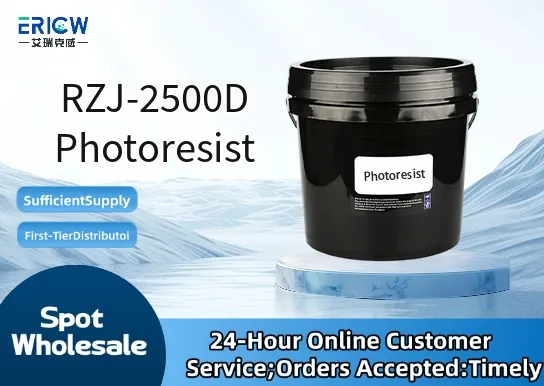
High-resolution patterning capability with sub-micron resolution (≤ 0.8 µm) under standard i-line (365 nm) exposure.
Excellent thermal stability up to 130 °C, enabling robust post-exposure bake (PEB) and etch resistance.
Low outgassing profile suitable for vacuum-compatible lithography processes and cleanroom Class 100 environments.
Optimized adhesion to silicon, SiO₂, and metal substrates without mandatory HMDS priming.
Consistent batch-to-batch performance verified via in-house GPC and UV-Vis spectral fingerprinting.
Microelectromechanical systems (MEMS) fabrication requiring high aspect ratio structures.
Power semiconductor device patterning (e.g., IGBTs, MOSFETs) on 150–200 mm wafers.
Thin-film sensor manufacturing including pressure, temperature, and optical transducers.
Research & development lithography in university cleanrooms and pilot-line facilities.
Maskless direct-write lithography using DLP and laser scanning systems (375–405 nm).
| Chemical Type | Positive-tone novolac-diazonaphthoquinone (DNQ) photoresist |
| Product Form | Liquid solution in propylene glycol monomethyl ether acetate (PGMEA) |
| Appearance | Clear, pale yellow liquid, free of particulates and gels |
| Solids Content | 22.0 ± 0.5 wt% (by gravimetric analysis) |
| Viscosity (25 °C) | 3.8–4.2 cP (measured per ASTM D445) |
| Primary Applications | i-line (365 nm) photolithography for MEMS, power devices, and sensors |
| Key Features | High sensitivity (~40–60 mJ/cm²), low standing wave effect, minimal T-top formation |
| Regulatory Compliance | REACH SVHC-free; RoHS 3 compliant; no intentionally added PFAS |
| Common Compatible Systems | Suitability |
| Canon FPA-3000 i-line Stepper | Highly Recommended – Validated for full-field exposure at 0.5–1.2 µm line/space |
| EVG® 620 Mask Aligner | Highly Recommended – Optimized contact/proximity mode performance with <1% CD variation |
| ASML PAS 5500/300 i-line Scanner | Recommended – Requires minor focus offset calibration; compatible with standard track modules |
| Karlsuss ACS300 Coater/Developer Track | Suitable – Verified with standard process recipes; minor rinse time adjustment advised |
Q1: What is the CAS Registry Number for RZJ-2500D Photoresist?
A: RZJ-2500D is a proprietary multi-component formulation; individual CAS numbers are assigned to key constituents only — full formulation CAS is not assigned per IUPAC guidelines for complex mixtures.
Q2: What is the recommended coating thickness and spin speed range for 2-inch to 8-inch wafers?
A: For 1.0–1.2 µm dry film thickness: 3000–4000 rpm (2-inch), 2500–3500 rpm (4-inch), 2000–3000 rpm (6–8-inch); final thickness validated via ellipsometry per SEMI MF-1530.
Q3: How does RZJ-2500D compare to AZ® 4620 in terms of resolution and etch resistance?
A: RZJ-2500D achieves comparable resolution (≤ 0.8 µm) but offers ~25% higher plasma etch selectivity vs. SiO₂ in CF₄/O₂ chemistry, with reduced sidewall scumming due to optimized DNQ decomposition kinetics.
Q4: Is RZJ-2500D compliant with ISO 10993 or USP Class VI for biomedical microdevice applications?
A: Not certified for direct biological contact; it meets ISO 14644-1 Class 5 cleanroom handling standards and has passed extractables testing per USP <661.1>, but full biocompatibility validation requires end-user-specific leachables assessment.
Contact With Us:
E-mail: wangxingqiang@ericwchem.com
Have a Questions? Call Us:
Add:
Building A1, Jiete Industrial Park, Huangpu District, Guangzhou City, Guangdong Province, China