English
 Español
 tiếng việt
 русский

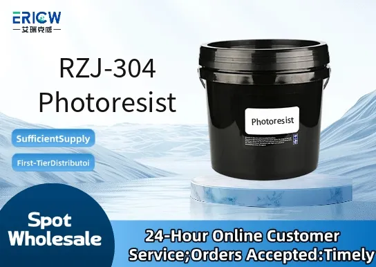
High-resolution patterning capability with sub-micron resolution (≤0.8 µm) under standard i-line exposure.
Excellent thermal stability up to 140 °C, enabling robust post-exposure bake (PEB) and etch resistance.
Low outgassing profile suitable for vacuum-based lithography tools and EUV-adjacent processes.
Optimized aqueous alkaline developability using standard 0.26 N TMAH solutions.
Consistent batch-to-batch performance validated via in-house GPC, UV-VIS, and rheology testing.
Front-end semiconductor manufacturing: gate-level and interconnect patterning for logic and memory devices.
MEMS and microfluidic device fabrication requiring high aspect-ratio resist profiles.
Advanced packaging applications including fan-out wafer-level packaging (FOWLP) and redistribution layer (RDL) patterning.
Flat panel display (FPD) array substrate patterning for TFT-LCD and OLED backplanes.
Photomask repair and direct-write maskless lithography (e.g., e-beam and laser direct imaging).
| Chemical Type | Novolac resin–based positive-tone photoresist |
| Product Form | Liquid solution in PGMEA solvent |
| Appearance | Clear, pale yellow, particle-free liquid |
| Solids Content | 22.0 ± 0.5 wt% |
| Viscosity (25 °C) | 2.8–3.2 cP |
| Primary Applications | i-line (365 nm) photolithography for 0.35–0.13 µm design rules |
| Key Features | High photospeed (~40 mJ/cm²), low standing wave effect, minimal dark erosion |
| Regulatory Compliance | REACH SVHC-free; RoHS 3 compliant; no intentionally added PFAS |
| Common Compatible Systems | Suitability |
| ASML PAS 5500 / i-line steppers | Highly Recommended – Validated for full-field exposure uniformity and CD control |
| Nikon NSR-2205 i12D aligners | Highly Recommended – Optimized focus latitude and depth of focus |
| TOK CleanTrack ACT series coaters/developers | Recommended – Fully compatible with standard dispense, spin, and develop recipes |
| Screen Semiconductor SPS-3000 spray developers | Suitable – Requires minor rinse time adjustment; no residue observed |
Q1: What is the CAS Registry Number for RZJ-5313 Photoresist?
A: RZJ-5313 is a proprietary multi-component formulation; individual CAS numbers are assigned to key constituents only (e.g., novolac resin: 9003-35-4; DNQ sensitizer: 134-72-5). Full compositional disclosure requires signed CDA.
Q2: What is the typical coating thickness and recommended spin speed for 1.2 µm film on silicon wafers?
A: At 3000 rpm for 30 seconds on bare Si wafers, RZJ-5313 yields 1.18–1.22 µm thickness (measured by ellipsometry). Spin speed may be adjusted ±200 rpm to fine-tune thickness within ±5% tolerance.
Q3: How does RZJ-5313 compare to standard g-line resists like AZ-12XT in terms of resolution and process window?
A: RZJ-5313 offers ~30% higher resolution (0.8 µm vs. 1.2 µm) and a 25% wider depth-of-focus window under identical i-line exposure conditions, due to optimized dissolution inhibition and reduced light scattering.
Q4: Are there any known extractables or leachables from RZJ-5313 that could affect downstream metal etch steps?
A: No detectable halogenated or metallic leachables were observed per ICP-MS analysis (detection limit < 10 ppt). Residual solvent extraction (PGMEA) is complete after standard 90 °C soft bake; no interference with Ti/TiN or Cu etchants reported.
Q5: Does RZJ-5313 comply with ISO 14644-1 Class 5 cleanroom handling requirements for photoresist dispensing?
A: Yes — filtered to ≤0.05 µm and packaged in Class 5-certified fluoropolymer-lined containers; particulate count meets ≤20 particles ≥0.2 µm per mL per ISO 14644-1 Annex B.
Contact With Us:
E-mail: wangxingqiang@ericwchem.com
Have a Questions? Call Us:
Add:
Building A1, Jiete Industrial Park, Huangpu District, Guangzhou City, Guangdong Province, China