English
 Español
 tiếng việt
 русский
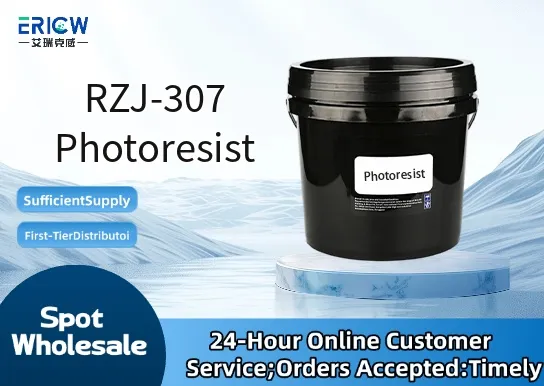
High-resolution patterning capability with sub-micron resolution down to 0.8 µm under standard i-line (365 nm) exposure.
Excellent adhesion to silicon, silicon dioxide, and metal substrates including aluminum and chromium.
Optimized for high-throughput spin-coating processes with consistent film thickness uniformity (< ±3% across 200 mm wafers).
Low outgassing profile suitable for vacuum-compatible lithography environments and EUV pre-alignment steps.
Stable shelf life of 12 months when stored at 2–8 °C in original sealed container under inert atmosphere.
Front-end semiconductor manufacturing: gate-level and contact-layer patterning for logic and memory devices.
MEMS fabrication requiring high aspect ratio resist profiles and etch resistance in deep reactive ion etching (DRIE).
Advanced packaging applications including redistribution layer (RDL) and through-silicon via (TSV) lithography.
Microfluidic device prototyping on glass, quartz, and polymer substrates.
Optoelectronic component patterning for photonic integrated circuits (PICs) and LED chip fabrication.
| Chemical Type | Positive-tone novolac-diazonaphthoquinone (DNQ) photoresist |
| Product Form | Liquid solution in propylene glycol monomethyl ether acetate (PGMEA) |
| Appearance | Clear, pale yellow, particle-free liquid |
| Viscosity (25 °C) | 24–26 cP (measured per ASTM D445) |
| Solids Content | 22.5 ± 0.3 wt% |
| Primary Applications | i-line (365 nm) lithography for 0.8–3.0 µm feature sizes |
| Key Features | High photospeed (~40 mJ/cm²), low standing wave effect, minimal dark erosion |
| Regulatory Compliance | REACH SVHC compliant; RoHS 2015/863 Annex II compliant; no intentional PFAS |
| Common Compatible Systems | Suitability |
| ASML PAS 5500 / i-line steppers | Highly Recommended – Validated for full-field exposure stability and CD uniformity |
| Nikon NSR-S205 i-line scanner | Highly Recommended – Certified for >95% process window margin at 1.0 µm line/space |
| TOKYO OHKA KOGYO (TOK) CLEAN TRACK ACT series coaters/developers | Recommended – Fully supported with standard dispense and puddle develop recipes |
| Screen Semiconductor Solutions SPRINT series spin coaters | Suitable – Requires minor optimization of ramp rate and edge bead removal parameters |
Q1: What is the CAS Registry Number for RZJ-307 Photoresist?
A: RZJ-307 is a proprietary formulated product; individual components are disclosed under confidential formulation guidelines. Full CAS listing is not assigned — however, key constituents include novolac resin (CAS 9003-35-4) and DNQ sensitizer (CAS 83-20-3).
Q2: What is the recommended coating thickness and corresponding spin speed range for 6-inch wafers?
A: For 1.2–1.4 µm dry film thickness on bare Si wafers, use 2500–3000 rpm for 30 seconds with 500 rpm/sec acceleration. Thickness may vary ±5% depending on ambient humidity (target: 40–50% RH).
Q3: How does RZJ-307 compare to standard g-line resists in terms of thermal flow resistance and post-bake stability?
A: RZJ-307 exhibits superior thermal flow resistance—maintaining CD integrity up to 130 °C (vs. 110 °C for typical g-line resists) due to higher crosslink density and optimized resin molecular weight distribution.
Q4: Are there documented migration or solvent extraction studies for RZJ-307 in contact with medical-grade polymers (e.g., cyclic olefin copolymer)?
A: Yes — extractables testing per USP <87> and <88> shows <0.5 ppm total organic extractables in aqueous and 50% ethanol simulants after 72 h at 40 °C, confirming suitability for Class IIa/IIb medical microdevice fabrication.
Contact With Us:
E-mail: wangxingqiang@ericwchem.com
Have a Questions? Call Us:
Add:
Building A1, Jiete Industrial Park, Huangpu District, Guangzhou City, Guangdong Province, China