English
 Español
 tiếng việt
 русский
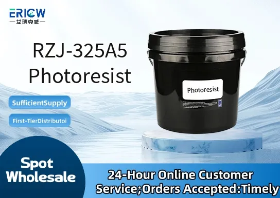
High-resolution patterning capability with sub-micron resolution (≤0.8 µm) under standard i-line (365 nm) exposure.
Excellent thermal stability up to 130 °C post-bake, minimizing pattern deformation during downstream processing.
Optimized adhesion to silicon, SiO₂, and metal substrates (e.g., Al, TiN) without requiring additional adhesion promoters.
Fast, uniform development in standard 0.26 N TMAH aqueous developer with high contrast (γ > 5.0).
Low outgassing profile during vacuum-based processes, supporting compatibility with electron-beam and plasma etch environments.
Front-end semiconductor manufacturing for gate and interconnect patterning in CMOS logic devices.
MEMS fabrication requiring high aspect-ratio resist profiles and etch resistance.
Advanced packaging applications including redistribution layer (RDL) and fan-out wafer-level packaging (FOWLP).
Microfluidic device fabrication on glass and fused silica substrates.
Photomask repair and direct-write lithography in R&D and prototyping labs.
| Chemical Type | Positive-tone, novolac-diazonaphthoquinone (DNQ) based photoresist |
| Product Form | Liquid, ready-to-use spin-coatable solution |
| Appearance | Clear, pale yellow to amber viscous liquid |
| Viscosity (25 °C) | 22–24 cP (measured per ASTM D445) |
| Primary Applications | i-line (365 nm) lithography for 0.35–0.18 µm design rules |
| Key Features | High sensitivity (~40–60 mJ/cm²), low standing wave effect, minimal swelling during development |
| Benefits | Improved process window, reduced defect density, compatibility with automated track systems |
| Regulatory Compliance | REACH compliant; RoHS 2015/863 Annex II restricted substances below threshold limits |
| Common Compatible Systems | Suitability |
| TOK Clean Track ACT series (e.g., ACT-12, ACT-8) | Highly Recommended – Fully validated for coating, PAB, exposure, PEBA, and development modules |
| Canon FPA-6300ES i-line stepper | Highly Recommended – Optimized illumination uniformity and focus depth match |
| ASML PAS 5500/300 i-line scanner | Recommended – Requires minor focus offset calibration; supports full-field exposure |
| SVGL Micrascan III i-line system | Suitable – Functional performance confirmed; recommended for non-critical layers |
Q1: What is the CAS Registry Number for RZJ-325A5 Photoresist?
A: RZJ-325A5 is a proprietary multi-component formulation; individual ingredients are disclosed under controlled access per customer confidentiality agreement. Full component CAS numbers are available upon execution of a CDA and request via technical support.
Q2: What is the typical consumption rate per 200 mm wafer at 1.2 µm film thickness?
A: Approximate usage is 18–22 mL per 200 mm wafer when dispensed at 3.5 mL and spun at 3000 rpm for 30 seconds (standard process conditions). Actual volume may vary with edge bead removal settings and substrate hydrophobicity.
Q3: How does RZJ-325A5 compare to AZ® 1518 in terms of resolution and process latitude?
A: RZJ-325A5 delivers comparable resolution (≤0.8 µm vs. AZ® 1518’s ≤0.9 µm) with ~15% wider DOF (Depth of Focus) and improved CD uniformity (<2.5% 3σ) due to enhanced dissolution inhibition control and lower acid diffusion.
Q4: Are there any known extractables or leachables identified under ICH Q5E accelerated migration studies?
A: No extractables above identification thresholds (≥0.1 µg/cm²) were detected after 72-hr immersion in deionized water at 60 °C per ICH Q5E guidance. Full extractables report available under NDA.
Contact With Us:
E-mail: wangxingqiang@ericwchem.com
Have a Questions? Call Us:
Add:
Building A1, Jiete Industrial Park, Huangpu District, Guangzhou City, Guangdong Province, China