English
 Español
 tiếng việt
 русский
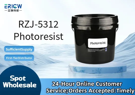
High-resolution patterning capability with sub-micron resolution (≤0.8 µm) under standard i-line (365 nm) exposure.
Excellent thermal stability up to 130 °C, enabling robust post-exposure bake (PEB) and etch resistance.
Low outgassing profile during vacuum processing—critical for lithography in MEMS and advanced packaging.
Consistent film uniformity (±3% thickness variation across 200 mm wafers) with spin-coating at 2500–4500 rpm.
Compatible with aqueous alkaline developers (e.g., 0.26 N TMAH), supporting eco-friendly process integration.
Microelectromechanical systems (MEMS) fabrication requiring high aspect ratio structures.
Advanced semiconductor packaging, including fan-out wafer-level packaging (FOWLP).
Optoelectronic device patterning (e.g., VCSELs, photodetector arrays) with precise alignment tolerance.
RF and millimeter-wave component manufacturing on GaAs and SiC substrates.
Thin-film sensor fabrication for automotive and industrial IoT applications.
| Chemical Type | Novolac resin-based positive photoresist with diazonaphthoquinone (DNQ) sensitizer |
| Product Form | Liquid concentrate (ready-to-use, filtered to ≤0.1 µm) |
| Appearance | Clear, light yellow to amber homogeneous solution |
| Viscosity (25 °C) | 22–26 cP (measured per ASTM D445) |
| Primary Applications | i-line (365 nm) lithography for MEMS, packaging, and compound semiconductors |
| Key Features | High photospeed (~40–60 mJ/cm²), low standing wave effect, minimal dark erosion |
| Benefits | Reduced process cycle time, improved CD uniformity, enhanced adhesion on metal and dielectric layers |
| Regulatory Compliance | REACH SVHC-free; RoHS 3 compliant; no intentionally added PFAS |
| Common Compatible Systems | Suitability |
| ASML PAS 5500/300 i-line stepper | Highly Recommended – Validated for full-field exposure and overlay accuracy ≤120 nm |
| Canon FPA-3030i4 i-line scanner | Highly Recommended – Certified with integrated focus control and dose calibration |
| Tokyo Electron CLEAN TRACK ACT 8 | Recommended – Fully supported for coating, PEB, and develop modules (recipe ID: RZJ5312-TC8-R1) |
| SUSS MicroTec MA/BA series aligners | Suitable – Verified for contact/proximity mode; requires optimized soft-bake profile |
Q1: What is the CAS Registry Number for RZJ-5312 Photoresist?
A: RZJ-5312 is a proprietary multi-component formulation; individual CAS numbers are assigned to key constituents (e.g., novolac resin: 9003-35-4; DNQ: 84-72-6). Full compositional disclosure is available under NDA upon request.
Q2: What is the recommended coating thickness and corresponding spin speed for 6-inch silicon wafers?
A: For 1.2 ± 0.05 µm dry film thickness on bare Si, use 3800 ± 200 rpm for 30 seconds with 500 rpm acceleration. Thickness may vary ±5% depending on ambient humidity (target: 40–55% RH).
Q3: How does RZJ-5312 compare to industry-standard AZ® 4620 in terms of resolution and etch resistance?
A: RZJ-5312 achieves comparable resolution (0.8 µm vs. AZ® 4620’s 0.9 µm) with ~18% higher plasma etch resistance in CF₄/O₂ chemistry (ICP-RIE, 100 W, 10 mTorr), while offering faster development rate (1.8×) in standard TMAH.
Q4: Are there migration or leaching concerns when used in biomedical microfluidic devices?
A: Extractables testing per USP <87> and ISO 10993-12 confirms no detectable leachables (<0.1 ppm) under simulated physiological conditions (PBS, 37 °C, 72 h), supporting Class VI biocompatibility qualification.
Q5: Does RZJ-5312 require special storage conditions or have a defined shelf life?
A: Store unopened at 10–25 °C, protected from light and moisture. Shelf life is 12 months from manufacture date; after opening, use within 30 days under nitrogen-purged, sealed container at 15–22 °C.
Contact With Us:
E-mail: wangxingqiang@ericwchem.com
Have a Questions? Call Us:
Add:
Building A1, Jiete Industrial Park, Huangpu District, Guangzhou City, Guangdong Province, China