English
 Español
 tiếng việt
 русский
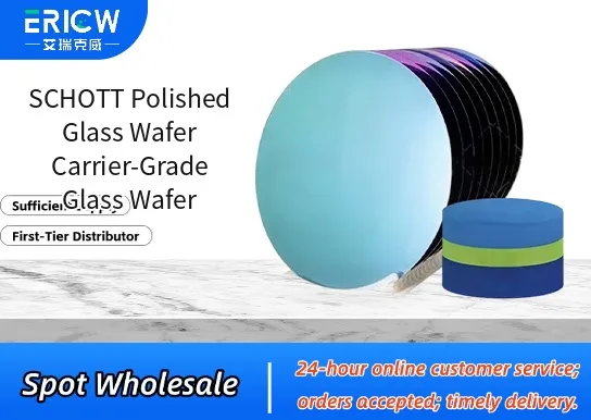
Ultra-flat, double-side polished surface with ≤0.1 nm RMS roughness for precision lithography and metrology.
High-purity borosilicate glass composition (e.g., SCHOTT BOROFLOAT® 33 equivalent) ensuring exceptional thermal stability and chemical resistance.
Low intrinsic birefringence and high optical homogeneity (Δn < 5 × 10⁻⁶), critical for advanced photomask and EUV mask blank applications.
Carrier-grade dimensional tolerances: thickness uniformity ±0.5 µm over full wafer area; total thickness variation (TTV) < 0.8 µm.
Controlled surface defect density (< 0.1 defects/cm² ≥0.3 µm) verified per SEMI Standard F78 and ISO 14644-1 Class 10 cleanroom handling.
Photomask blanks for deep ultraviolet (DUV) and extreme ultraviolet (EUV) lithography in semiconductor front-end manufacturing.
Substrates for reticle inspection systems, mask repair tools, and automated optical inspection (AOI) platforms.
Reference wafers in semiconductor process control, overlay metrology, and scanner calibration.
High-precision optics carriers in vacuum-compatible metrology chambers and wafer-level testing equipment.
Base substrates for thin-film deposition of Cr, MoSi, or multilayer EUV reflective coatings.
| Chemical Type | Borosilicate glass (Al₂O₃–B₂O₃–SiO₂ system, low-alkali) |
| Product Form | Circular wafer, double-side polished, edge-isolated bevel |
| Standard Diameters | 150 mm, 200 mm, 300 mm (custom sizes available) |
| Thickness Options | 2.0 mm, 3.2 mm, 6.35 mm (±0.5 µm tolerance) |
| Surface Finish | Double-side polished; Ra < 0.2 nm, TTV < 0.8 µm |
| Thermal Expansion Coefficient (20–300 °C) | 3.25 × 10⁻⁶ /K |
| Melting Point (Softening Point) | ≈820 °C (annealing point); no defined sharp melting point |
| Regulatory Compliance | RoHS 2015/863 compliant; REACH SVHC-free; ISO 9001 & ISO 14001 certified manufacturing |
| Common Compatible Systems | Suitability |
| KLA-Tencor 8 Series Mask Inspection Tools | Highly Recommended – Optimized flatness and particle performance validated per KLA Tool Spec M8-PS-001 |
| ASML PAS 5500/300 Photomask Steppers | Highly Recommended – Meets ASML reticle stage Z-height and thermal drift requirements |
| Applied Materials UVision™ Reticle Cleaning Systems | Recommended – Resists aggressive UV/ozone and megasonic cleaning cycles without haze formation |
| Nikon NSR-S630D Mask Aligners | Suitable – Verified compatibility with vacuum chucks and alignment fiducials |
Q1: Does this product have a CAS Registry Number?
A: No — as an engineered inorganic glass substrate (not a chemical compound), it does not have a CAS number. Composition is defined by proprietary SCHOTT glass formulation specifications (e.g., BOROFLOAT® 33 equivalent), documented in Material Compliance Dossier.
Q2: What is the recommended handling protocol to prevent surface contamination or micro-scratching?
A: Use Class 10 cleanroom protocols: handle only with powder-free nitrile gloves; transport in SMIF pods or FOUPs with PTFE-coated carriers; avoid contact with metal tweezers—use ceramic or carbon-fiber vacuum wands calibrated to < 50 g force.
Q3: How does this carrier-grade wafer compare to standard float glass wafers in terms of thermal budget for coating processes?
A: It supports sustained processing up to 450 °C (e.g., Cr adhesion layer annealing) with < 0.02% dimensional drift — versus > 0.15% drift observed in soda-lime float glass — due to its lower CTE and higher strain point (≈640 °C).
Q4: Are extractables or leachables a concern during wet cleaning or plasma etch steps?
A: No measurable alkali or boron leaching occurs under standard semiconductor cleaning (SC1, SC2, dilute HF) or O₂/Ar plasma exposure, confirmed via ICP-MS analysis per SEMI F57 guidelines (< 0.05 ng/cm² Na⁺, < 0.02 ng/cm² B³⁺).
Contact With Us:
E-mail: wangxingqiang@ericwchem.com
Have a Questions? Call Us:
Add:
Building A1, Jiete Industrial Park, Huangpu District, Guangzhou City, Guangdong Province, China