English
 Español
 tiếng việt
 русский
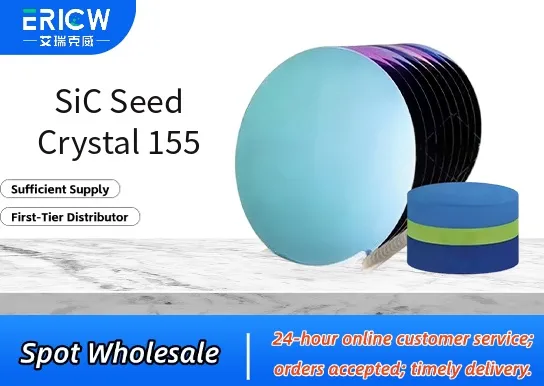
High-purity single-crystal silicon carbide (≥99.999% SiC) with controlled 4H polytype dominance.
Optimized surface flatness (Ra < 0.3 nm) and low microroughness for reliable epitaxial nucleation.
Consistent crystallographic orientation (c-axis normal, ±0.1° off-axis tolerance) ensuring uniform growth initiation.
Low dislocation density (< 500 cm⁻²) verified by KOH etch pit density (EPD) analysis.
Thermally stable up to 2200 °C in inert or vacuum environments without decomposition or phase segregation.
Substrate for homoepitaxial growth of high-voltage SiC power devices (MOSFETs, Schottky diodes).
Seed material in physical vapor transport (PVT) crystal growth furnaces for bulk SiC boule production.
Reference standard in R&D labs for SiC crystal quality benchmarking and process validation.
Base wafer for advanced heterostructure integration in wide-bandgap semiconductor research.
Calibration component in high-temperature XRD and synchrotron-based structural characterization setups.
| Chemical Type | Silicon Carbide (SiC), 4H polytype dominant |
| Product Form | Polished single-crystal wafer (free-standing) |
| Standard Diameter | 155 mm (6-inch equivalent) |
| Thickness | 1.0 ± 0.05 mm |
| Crystal Orientation | c-plane (0001), 4° off-axis toward [11–20] |
| Surface Finish | Double-side polished, epi-ready (Ra < 0.3 nm) |
| Primary Applications | Homoepitaxial seed for PVT and sublimation growth |
| Regulatory Compliance | RoHS 2015/863 compliant; REACH SVHC-free declaration available |
| Common Compatible Systems | Suitability |
| IKZ PVT Furnace Series (e.g., PVT-1200, PVT-1500) | Highly Recommended – Designed for 155 mm seed geometry and thermal profile matching |
| SCIOCS Sublimation Growth System (SGS-6i) | Highly Recommended – Verified compatibility with 4H-SiC seed alignment and graphite fixture interface |
| Aixtron HT-CVD Reactor (with SiC adaptation kit) | Recommended – Requires custom carrier plate; supports seed pre-heating protocol |
| Kyocera Advanced Crystal Growth Platform (K-ACG-155) | Suitable – Compatible with mechanical clamping and IR pyrometry calibration |
Q1: What is the CAS Registry Number for SiC Seed Crystal 155?
A: Silicon carbide as a compound has CAS No. 409-21-2; however, SiC Seed Crystal 155 is a manufactured crystalline product — not a chemical substance per se — and therefore does not carry a unique CAS number. Batch-specific CoA and traceability documentation are provided with each shipment.
Q2: Is there a recommended minimum usage temperature or ramp rate when loading into a PVT furnace?
A: Yes. Preheat the seed to ≥800 °C under inert gas (Ar or N₂) before introducing to high-temperature zone; recommended ramp rate ≤10 °C/min below 1200 °C to minimize thermal stress-induced microcracking.
Q3: How does SiC Seed Crystal 155 differ from standard SiC substrates used for device fabrication?
A: Unlike device-grade wafers, SiC Seed Crystal 155 features enhanced axial symmetry, ultra-low EPD, and optimized off-cut geometry specifically for bulk crystal propagation — not direct device processing. It lacks device-layer doping or metallization and undergoes stricter thermal history screening.
Q4: Are there any known extractables or leachables under high-temperature vacuum conditions?
A: No measurable volatile species (e.g., SiO, C₂, Si₂C) are observed below 2000 °C in high-vacuum (<10⁻⁵ mbar) environments. Residual surface carbon or silicon oxide contaminants are removed via in-situ H₂ annealing prior to growth — confirmed by residual gas analysis (RGA) data included in technical dossiers.
Contact With Us:
E-mail: wangxingqiang@ericwchem.com
Have a Questions? Call Us:
Add:
Building A1, Jiete Industrial Park, Huangpu District, Guangzhou City, Guangdong Province, China