English
 Español
 tiếng việt
 русский
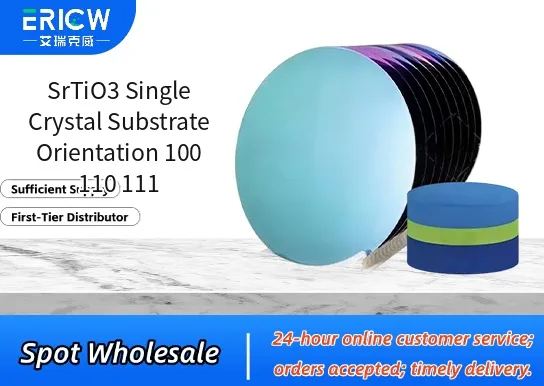
High-purity single-crystal structure with low defect density and excellent surface flatness (Ra < 0.2 nm).
Precisely controlled crystallographic orientation: available in (100), (110), and (111) surface normals with ±0.5° miscut tolerance.
Chemically stable perovskite lattice, resistant to thermal decomposition up to 1400 °C in inert or oxidizing atmospheres.
Excellent dielectric properties (εᵣ ≈ 300 at 1 kHz, 25 °C) and low dielectric loss (tan δ < 0.001).
Atomically clean, polished surfaces suitable for epitaxial thin-film growth without additional chemical etching.
Heteroepitaxial growth of high-temperature superconductors (e.g., YBCO, LSCO) and complex oxide heterostructures.
Substrate for ferroelectric and multiferroic thin films (e.g., BiFeO₃, PZT) in memory and sensor devices.
Platform for two-dimensional electron gas (2DEG) studies at LaAlO₃/SrTiO₃ interfaces.
Reference substrate in X-ray diffraction (XRD), RHEED, and surface science calibration experiments.
Base material for tunable microwave dielectric components and integrated oxide-based electronics.
| Chemical Type | Strontium Titanate (SrTiO₃), perovskite oxide |
| Product Form | Polished single-crystal wafer (double-side polished, EPI-ready) |
| Appearance | Transparent, colorless to pale yellow, mirror-like surface |
| Melting Point | ≈ 2080 °C (decomposes above 1600 °C in air; stable under controlled annealing) |
| Primary Applications | Epitaxial oxide thin-film deposition, fundamental condensed matter research, device prototyping |
| Key Features | Low dislocation density (< 1 × 10⁴ cm⁻²), uniform lattice parameter (a = 3.905 Å), stoichiometric composition |
| Benefits | Enables reproducible interface engineering, minimizes interfacial strain, supports atomic-layer-resolved growth |
| Regulatory Compliance | RoHS-compliant; no REACH SVHC substances above threshold; SDS available upon request |
| Common Compatible Systems | Suitability |
| Pulsed Laser Deposition (PLD) | Highly Recommended – Optimal for stoichiometric transfer of complex oxides at 600–800 °C |
| Molecular Beam Epitaxy (MBE) | Recommended – Requires in-situ oxygen partial pressure control and elevated substrate temperature |
| Sputtering (RF & DC Magnetron) | Suitable – Compatible with reactive sputtering using O₂/Ar mixtures; post-annealing often beneficial |
| Atomic Layer Deposition (ALD) | Recommended – Supports nucleation of Al₂O₃, HfO₂, and other gate oxides with precise interfacial control |
Q1: What is the CAS Registry Number for SrTiO₃?
A: The CAS number for strontium titanate is 12060-58-1.
Q2: Is SrTiO₃ substrate suitable for direct use in aqueous or acidic environments?
A: No — SrTiO₃ is not chemically inert in low-pH solutions; it may undergo slow strontium leaching. For wet processing, brief deionized water rinse is acceptable; prolonged exposure to acids or chelators is not recommended.
Q3: How does SrTiO₃ (100) compare to MgO or LaAlO₃ substrates for oxide epitaxy?
A: SrTiO₃ (100) offers superior lattice match to many functional oxides (e.g., 0.2% mismatch with YBCO), lower interfacial reactivity than MgO, and better thermal expansion compatibility than LaAlO₃ — resulting in reduced cracking and improved film quality.
Q4: Does this product comply with EU REACH and US TSCA regulations?
A: Yes — SrTiO₃ is listed on both the TSCA Inventory and ECHA’s REACH registered substances list; our material contains no intentionally added nanomaterials or restricted impurities above reporting thresholds.
Q5: Can SrTiO₃ substrates be reused after thin-film growth?
A: Reuse is technically possible only after rigorous cleaning (e.g., piranha + HF dip + annealing), but surface reconstruction and residual contamination typically compromise epitaxial quality; we recommend single-use for critical applications.
Contact With Us:
E-mail: wangxingqiang@ericwchem.com
Have a Questions? Call Us:
Add:
Building A1, Jiete Industrial Park, Huangpu District, Guangzhou City, Guangdong Province, China