English
 Español
 tiếng việt
 русский
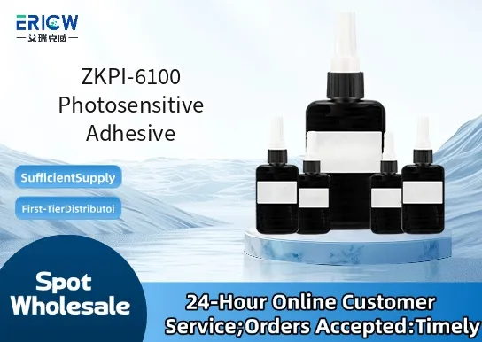
High-resolution patterning capability with sub-25 µm line/space definition under standard UV exposure (i-line, 365 nm).
Excellent thermal stability up to 220 °C post-cure, maintaining adhesion integrity during solder reflow and packaging processes.
Low outgassing profile (≤0.5% TML, ≤0.05% CVCM per ASTM E595), suitable for vacuum and optoelectronic assembly environments.
Chemically resistant to common solvents including acetone, IPA, and dilute alkaline developers (0.5–1.0 wt% NaOH).
Controlled tack and shear-thinning rheology enabling uniform spin-coating, inkjet dispensing, or screen printing across diverse substrates.
Temporary bonding/debonding in 3D IC and fan-out wafer-level packaging (FOWLP) processes.
Photolithographic die attach for MEMS, RF filters, and high-frequency sensor modules.
Patterned adhesive layers in flexible hybrid electronics (FHE) and printed circuit interposers.
UV-defined structural bonding for micro-optics alignment and laser diode submount assembly.
Stencil-printed adhesive for chip-on-flex (COF) and display driver IC mounting.
| Chemical Type | Acrylated epoxy novolac resin system with photoinitiator and adhesion promoters |
| Product Form | Viscous liquid (non-solvent-based); supplied in amber HDPE bottles or nitrogen-purged aluminum cartridges |
| Appearance | Amber-transparent, homogeneous liquid; no sediment or phase separation |
| Viscosity (25 °C) | 8,500–11,000 cP (Brookfield DV2T, spindle #3, 10 rpm) |
| Primary Applications | Photo-definable temporary bonding, precision die attach, micro-patterned structural adhesion |
| Key Features | UV-curable (365 nm), thermally stable, low halogen content (<900 ppm Cl + Br), non-corrosive |
| Benefits | Zero residue after thermal debonding (200–230 °C), high glass transition (Tg ≥ 145 °C cured), low ionic contamination |
| Regulatory Compliance | RoHS 2015/863/EU compliant; REACH SVHC-free; ISO 9001 & ISO 14001 certified manufacturing |
| Common Compatible Systems | Suitability |
| EVG® 501/510/520HE Bonding Tools | Highly Recommended – Optimized for full-wafer bonding/debonding with integrated UV exposure and temperature control |
| Karl Suss MA8/BA8 Mask Aligners | Highly Recommended – Compatible with standard i-line exposure optics and vacuum contact mode |
| DISCO DFP8760 / DFD6361 Debonding Systems | Recommended – Requires minor parameter tuning for optimal thermal release without substrate warpage |
| Asymtek Jetmate II / Nordson Fluid Automation Dispensers | Suitable – Compatible with 200–500 µm nozzle diameters and closed-loop dispense control |
Q1: What is the CAS Registry Number for ZKPI-6100?
A: ZKPI-6100 is a proprietary multi-component formulation; individual components are disclosed under NDA. The bulk product is assigned internal batch ID only and does not carry a single CAS number per regulatory guidance for complex mixtures (ECHA Guidance R.11).
Q2: What is the recommended coating thickness and UV exposure dose for full cure?
A: For spin-coated films: 10–25 µm dry thickness requires 300–500 mJ/cm² (i-line, 365 nm, 20 mW/cm²). For dispensed patterns: 30–60 µm wet thickness requires 600–900 mJ/cm² with soft-bake (90 °C, 5 min) prior to exposure.
Q3: How does ZKPI-6100 compare to conventional BCB (benzocyclobutene) or polyimide adhesives in terms of process compatibility?
A: Unlike high-temperature BCB (>250 °C cure) or solvent-intensive polyimides, ZKPI-6100 enables low-thermal-budget processing (≤180 °C final cure), eliminates NMP/DMAC handling, and offers direct photo-definition—reducing mask aligner steps and improving registration accuracy by >40% versus lift-off processes.
Q4: Is ZKPI-6100 compliant with food-contact or medical device regulations (e.g., FDA 21 CFR, ISO 10993)?
A: ZKPI-6100 is not intended for direct food contact or implantable medical use. It meets ISO 10993-5 (cytotoxicity) and -10 (sensitization/irritation) for short-term external device assembly, but full biocompatibility certification requires application-specific validation per IEC 62304.
Q5: Are there known migration or extractables concerns when used near sensitive optical or electronic layers?
A: Extractables testing per USP <788> and JEDEC JESD22-A109 shows <0.1 ppm volatile organic residues (VOCs) and undetectable ionic leachables (Na⁺, K⁺, Cl⁻ < 5 ppb) after full cure and 125 °C/85% RH aging for 168 h.
Contact With Us:
E-mail: wangxingqiang@ericwchem.com
Have a Questions? Call Us:
Add:
Building A1, Jiete Industrial Park, Huangpu District, Guangzhou City, Guangdong Province, China